STM32F302xx/STM32F303xx
Electrical characteristics
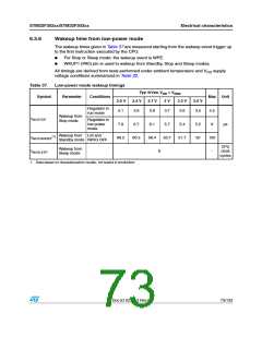
6.3.6
Wakeup time from low-power mode
The wakeup times given in Table 37 are measured starting from the wakeup event trigger up
to the first instruction executed by the CPU:
●
For Stop or Sleep mode: the wakeup event is WFE.
●
WKUP1 (PA0) pin is used to wakeup from Standby, Stop and Sleep modes.
All timings are derived from tests performed under ambient temperature and V supply
DD
voltage conditions summarized in Table 22.
Table 37. Low-power mode wakeup timings
Typ @VDD, VDD = VDDA
Symbol
Parameter
Conditions
Max Unit
2.0 V
2.4 V
2.7 V
3 V
3.3 V
3.6 V
Regulator in
run mode
4.1
3.9
3.8
3.7
3.6
3.5
4.5
Wakeup from
Stop mode
tWUSTOP
Regulator in
low power
mode
7.9
6.7
6.1
5.7
5.4
5.2
50
9
100
-
µs
Wakeup from LSI and
Standby mode IWDG OFF
(1)
tWUSTANDBY
69.2
60.3
56.4
53.7
51.7
CPU
clock
Wakeup from
Sleep mode
tWUSLEEP
6
cycles
1. Data based on characterization results, not tested in production.
Doc ID 023353 Rev 5
73/133

 STMICROELECTRONICS [ ST ]