STA335BW
Register description
5.6
Configuration register F (address 0x05)
D7
D6
D5
D4
D3
D2
D1
D0
EAPD
0
PWDN
1
ECLE
0
LDTE
1
BCLE
1
IDE
1
OCFG1
0
OCFG0
0
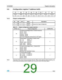
5.6.1
Output configuration
Bit
R/W
RST
Name
Description
Selects the Output Configuration
0
1
R/W
R/W
0
0
OCFG0
OCFG1
Table 14. Output configuration engine selection
OCFG(1..0)
Output configuration
CONFIG PIN
2 Channel (Full-Bridge) Power, 2 Channel Data-Out:
1A/1B →1A/1B
2A/2B →2A/2B
LineOut1 →3A/3B
LineOut2 →4A/4B
Line Out Configuration determined by LOC register
00
0
0
2(Half-Bridge).1(Full-Bridge) On-Board Power:
1A →1A
2A →1B
3A/3B →2A/2B Binary 45°
Binary 0 °
Binary 90°
01
1A/B →3A/B
2A/B →4A/B
Binary 0°
Binary 90°
2 Channel (Full-Bridge) Power, 1 Channel DDX:
1A/1B →1A/1B
10
11
2A/2B →2A/2B
3A/3B →3A/3B
EAPDEXT and TWARNEXT Active
0
1
1 Channel Mono-Parallel:
3A →1A/1B
3B →2A/2B
w/ C3BO 45°
w/ C3BO 45°
1A/1B →3A/3B
2A/2B →4A/4B
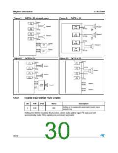
Note:
To the left of the arrow is the processing channel. When using channel output mapping, any
of the three processing channel outputs can be used for any of the three inputs.
29/54

 STMICROELECTRONICS [ ST ]