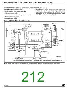
MULTIPROTOCOL SERIAL COMMUNICATIONS INTERFACE (SCI-M)
MULTIPROTOCOL SERIAL COMMUNICATIONS INTERFACE (Cont’d)
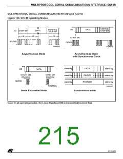
10.5.4 SCI-M Operating Modes
10.5.4.1 Asynchronous Mode
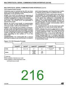
10.5.4.2
Asynchronous
Mode
with
Synchronous Clock
In this mode, data and clock are synchronous,
each data bit is sampled once per clock period.
In this mode, data and clock can be asynchronous
(the transmitter and receiver can use their own
clocks to sample received data), each data bit is
sampled 16 times per clock period.
For transmit operation, a general purpose I/O port
pin can be programmed to output the CLKOUT
signal from the baud rate generator. If the SCI is
provided with an external transmission clock
source, there will be a skew equivalent to two
INTCLK periods between clock and data.
The baud rate clock should be set to the ÷16 Mode
and the frequency of the input clock (from an ex-
ternal source or from the internal baud-rate gener-
ator output) is set to suit.
Data will be transmitted on the falling edge of the
transmit clock. Received data will be latched into
the SCI on the rising edge of the receive clock.
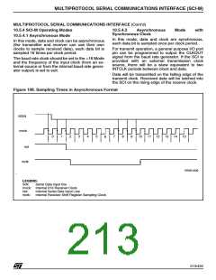
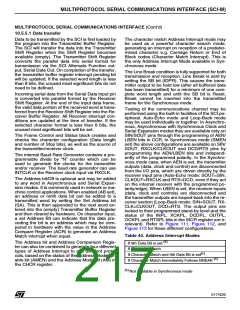
Figure 108. Sampling Times in Asynchronous Format
SDIN
rcvck
0
1
2
3
4
5
7
8
9
10
11 12
13
14
15
rxd
rxclk
VR001409
LEGEND:
Serial Data Input line
rcvck: Internal X16 Receiver Clock
SIN:
Internal Serial Data Input Line
Internal Receiver Shift Register Sampling Clock
rxd:
rxclk:
213/426
9

 STMICROELECTRONICS [ ST ]