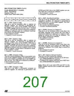
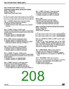
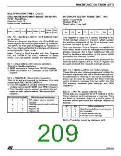
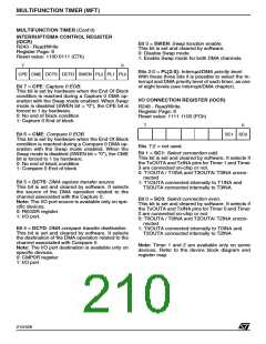
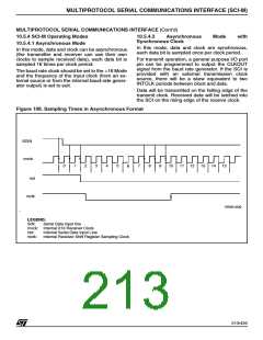
MULTIPROTOCOL SERIAL COMMUNICATIONS INTERFACE (SCI-M)
10.5 MULTIPROTOCOL SERIAL COMMUNICATIONS INTERFACE (SCI-M)
10.5.1 Introduction
■ Programmable address indication bit (wake-up
bit) and user invisible compare logic to support
multiple microcomputer networking. Optional
character search function.
The Multiprotocol Serial Communications Inter-
face (SCI-M) offers full-duplex serial data ex-
change with a wide range of external equipment.
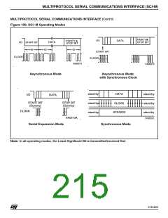
The SCI-M offers four operating modes: Asynchro-
nous, Asynchronous with synchronous clock, Seri-
al expansion and Synchronous.
■ Internal diagnostic capabilities:
– Local loopback for communications link fault
isolation.
– Auto-echo for communications link fault isola-
tion.
10.5.2 Main Features
■ Full duplex synchronous and asynchronous
operation.
■ Separate interrupt/DMA channels for transmit
and receive.
■ Transmit, receive, line status, and device
address interrupt generation.
■ In addition, a Synchronous mode supports:
■ Integral Baud Rate Generator capable of
– High speed communication
– Possibility of hardware synchronization (RTS/
DCD signals).
– Programmable polarity and stand-by level for
data SIN/SOUT.
– Programmable active edge and stand-by level
for clocks CLKOUT/RXCL.
– Programmable active levels of RTS/DCD sig-
nals.
– Full Loop-Back and Auto-Echo modes for DA-
TA, CLOCKs and CONTROLs.
dividing the input clock by any value from 2 to
16
2 -1 (16 bit word) and generating the internal
16X data sampling clock for asynchronous
operation or the 1X clock for synchronous
operation.
■ Fully programmable serial interface:
– 5, 6, 7, or 8 bit word length.
– Even, odd, or no parity generation and detec-
tion.
– 0, 1, 1.5, 2, 2.5, 3 stop bit generation.
– Complete status reporting capabilities.
– Line break generation and detection.
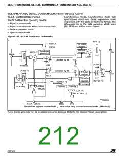
Figure 106. SCI-M Block Diagram
ST9 CORE BUS
DMA
CONTROLLER
DMA
CONTROLLER
TRANSMIT
BUFFER
REGISTER
ADDRESS
COMPARE
REGISTER
RECEIVER
BUFFER
REGISTER
RECEIVER
SHIFT
REGISTER
TRANSMIT
SHIFT
REGISTER
Frame Control
and STATUS
CLOCK and
BAUD RATE
GENERATOR
ALTERNATE
FUNCTION
VA00169A
SDS
SOUT RTS
TXCLK/CLKOUT RXCLK DCD
SIN
211/426
9

 STMICROELECTRONICS [ ST ]