ST10F276E
List of figures
List of figures
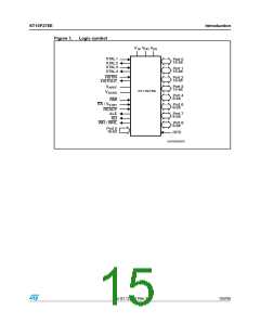
Figure 1.
Figure 2.
Figure 3.
Figure 4.
Figure 5.
Figure 6.
Figure 7.
Figure 8.
Figure 9.
Logic symbol. . . . . . . . . . . . . . . . . . . . . . . . . . . . . . . . . . . . . . . . . . . . . . . . . . . . . . . . . . . . 15
Pin configuration (top view) . . . . . . . . . . . . . . . . . . . . . . . . . . . . . . . . . . . . . . . . . . . . . . . . 16
Block diagram. . . . . . . . . . . . . . . . . . . . . . . . . . . . . . . . . . . . . . . . . . . . . . . . . . . . . . . . . . . 23
Flash modules structure . . . . . . . . . . . . . . . . . . . . . . . . . . . . . . . . . . . . . . . . . . . . . . . . . . . 24
ST10F276E new standard bootstrap loader program flow . . . . . . . . . . . . . . . . . . . . . . . . . 49
Booting steps for ST10F276E. . . . . . . . . . . . . . . . . . . . . . . . . . . . . . . . . . . . . . . . . . . . . . . 51
Hardware provisions to activate the BSL . . . . . . . . . . . . . . . . . . . . . . . . . . . . . . . . . . . . . . 52
Memory configuration after reset . . . . . . . . . . . . . . . . . . . . . . . . . . . . . . . . . . . . . . . . . . . . 53
UART bootstrap loader sequence . . . . . . . . . . . . . . . . . . . . . . . . . . . . . . . . . . . . . . . . . . . 55
Figure 10. Baud rate deviation between host and ST10F276E . . . . . . . . . . . . . . . . . . . . . . . . . . . . . . 58
Figure 11. CAN bootstrap loader sequence. . . . . . . . . . . . . . . . . . . . . . . . . . . . . . . . . . . . . . . . . . . . . 59
Figure 12. Bit rate measurement over a predefined zero-frame . . . . . . . . . . . . . . . . . . . . . . . . . . . . . 62
Figure 13. Reset boot sequence . . . . . . . . . . . . . . . . . . . . . . . . . . . . . . . . . . . . . . . . . . . . . . . . . . . . . 71
Figure 14. CPU Block Diagram (MAC Unit not included). . . . . . . . . . . . . . . . . . . . . . . . . . . . . . . . . . . 72
Figure 15. MAC unit architecture . . . . . . . . . . . . . . . . . . . . . . . . . . . . . . . . . . . . . . . . . . . . . . . . . . . . . 73
Figure 16. X-Interrupt basic structure . . . . . . . . . . . . . . . . . . . . . . . . . . . . . . . . . . . . . . . . . . . . . . . . . 81
Figure 17. Block diagram of GPT1. . . . . . . . . . . . . . . . . . . . . . . . . . . . . . . . . . . . . . . . . . . . . . . . . . . . 86
Figure 18. Block diagram of GPT2. . . . . . . . . . . . . . . . . . . . . . . . . . . . . . . . . . . . . . . . . . . . . . . . . . . . 88
Figure 19. Block diagram of PWM module . . . . . . . . . . . . . . . . . . . . . . . . . . . . . . . . . . . . . . . . . . . . . 89
Figure 20. Connection to single CAN bus via separate CAN transceivers . . . . . . . . . . . . . . . . . . . . 101
Figure 21. Connection to single CAN bus via common CAN transceivers. . . . . . . . . . . . . . . . . . . . . 102
Figure 22. Connection to two different CAN buses (e.g. for gateway application). . . . . . . . . . . . . . . 103
Figure 23. Connection to one CAN bus with internal Parallel Mode enabled . . . . . . . . . . . . . . . . . . 103
Figure 24. Asynchronous power-on RESET (EA = 1) . . . . . . . . . . . . . . . . . . . . . . . . . . . . . . . . . . . . 109
Figure 25. Asynchronous power-on RESET (EA = 0) . . . . . . . . . . . . . . . . . . . . . . . . . . . . . . . . . . . . 110
Figure 26. Asynchronous hardware RESET (EA = 1) . . . . . . . . . . . . . . . . . . . . . . . . . . . . . . . . . . . . 111
Figure 27. Asynchronous hardware RESET (EA = 0) . . . . . . . . . . . . . . . . . . . . . . . . . . . . . . . . . . . . 112
Figure 28. Synchronous short / long hardware RESET (EA = 1). . . . . . . . . . . . . . . . . . . . . . . . . . . . 114
Figure 29. Synchronous short / long hardware RESET (EA = 0). . . . . . . . . . . . . . . . . . . . . . . . . . . . 115
Figure 30. Synchronous long hardware RESET (EA = 1) . . . . . . . . . . . . . . . . . . . . . . . . . . . . . . . . . 116
Figure 31. Synchronous long hardware RESET (EA = 0) . . . . . . . . . . . . . . . . . . . . . . . . . . . . . . . . . 117
Figure 32. SW / WDT unidirectional RESET (EA = 1) . . . . . . . . . . . . . . . . . . . . . . . . . . . . . . . . . . . . 118
Figure 33. SW / WDT unidirectional RESET (EA = 0) . . . . . . . . . . . . . . . . . . . . . . . . . . . . . . . . . . . . 119
Figure 34. SW / WDT bidirectional RESET (EA = 1) . . . . . . . . . . . . . . . . . . . . . . . . . . . . . . . . . . . . . 121
Figure 35. SW / WDT bidirectional RESET (EA = 0) . . . . . . . . . . . . . . . . . . . . . . . . . . . . . . . . . . . . . 122
Figure 36. SW / WDT bidirectional RESET (EA = 0) followed by a HW RESET . . . . . . . . . . . . . . . . 123
Figure 37. Minimum external reset circuitry. . . . . . . . . . . . . . . . . . . . . . . . . . . . . . . . . . . . . . . . . . . . 124
Figure 38. System reset circuit . . . . . . . . . . . . . . . . . . . . . . . . . . . . . . . . . . . . . . . . . . . . . . . . . . . . . 125
Figure 39. Internal (simplified) reset circuitry . . . . . . . . . . . . . . . . . . . . . . . . . . . . . . . . . . . . . . . . . . . 125
Figure 40. Example of software or watchdog bidirectional reset (EA = 1) . . . . . . . . . . . . . . . . . . . . . 126
Figure 41. Example of software or watchdog bidirectional reset (EA = 0) . . . . . . . . . . . . . . . . . . . . . 127
Figure 42. PORT0 bits latched into the different registers after reset . . . . . . . . . . . . . . . . . . . . . . . . 130
Figure 43. External RC circuitry on RPD pin . . . . . . . . . . . . . . . . . . . . . . . . . . . . . . . . . . . . . . . . . . . 132
Figure 44. Port2 test mode structure . . . . . . . . . . . . . . . . . . . . . . . . . . . . . . . . . . . . . . . . . . . . . . . . . 183
Figure 45. Supply current versus the operating frequency (RUN and IDLE modes) . . . . . . . . . . . . . 184
Figure 46. A/D conversion characteristic . . . . . . . . . . . . . . . . . . . . . . . . . . . . . . . . . . . . . . . . . . . . . . 190
Figure 47. A/D converter input pins scheme . . . . . . . . . . . . . . . . . . . . . . . . . . . . . . . . . . . . . . . . . . . 192
Figure 48. Charge sharing timing diagram during sampling phase . . . . . . . . . . . . . . . . . . . . . . . . . . 193
Doc ID 12303 Rev 3
11/235

 STMICROELECTRONICS [ ST ]