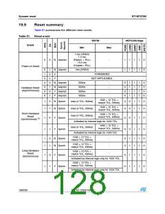
System reset
ST10F276E
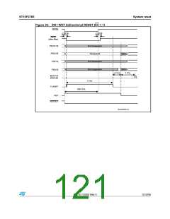
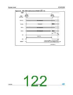
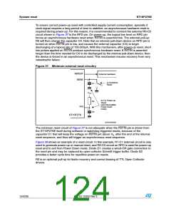
To ensure correct power-up reset with controlled supply current consumption, specially if
clock signal requires a long period of time to stabilize, an asynchronous hardware reset is
required during power-up. For this reason, it is recommended to connect the external R0-C0
circuit shown in Figure 37 to the RPD pin. On power-up, the logical low level on RPD pin
forces an asynchronous hardware reset when RSTIN is asserted low. The external pull-up
R0 will then charge the capacitor C0. Note that an internal pull-down device on RPD pin is
turned on when RSTIN pin is low, and causes the external capacitor (C0) to begin
discharging at a typical rate of 100-200μA. With this mechanism, after power-up reset, short
low pulses applied on RSTIN produce synchronous hardware reset. If RSTIN is asserted
longer than the time needed for C0 to be discharged by the internal pull-down device, then
the device is forced in an asynchronous reset. This mechanism insures recovery from very
catastrophic failure.
Figure 37. Minimum external reset circuitry
234/54
234).
%XTERNAL (ARDWARE
ꢑ
Aꢏ (ARDWARE
2ESET
#ꢀ
6
##
Bꢏ &OR 0OWERꢅUP
2ESET
ꢍAND )NTERRUPTIBLE
0OWER $OWN
MODEꢏ
2ꢉ
#ꢉ
20$
ꢑ
34ꢀꢉ&ꢁꢊꢄ
'!0'2)ꢉꢉꢈꢈꢀ
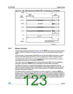
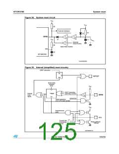
The minimum reset circuit of Figure 37 is not adequate when the RSTIN pin is driven from
the ST10F276E itself during software or watchdog triggered resets, because of the
capacitor C1 that will keep the voltage on RSTIN pin above VIL after the end of the internal
reset sequence, and thus will trigger an asynchronous reset sequence.
Figure 38 shows an example of a reset circuit. In this example, R1-C1 external circuit is only
used to generate power-up or manual reset, and R0-C0 circuit on RPD is used for power-up
reset and to exit from Power Down mode. Diode D1 creates a wired-OR gate connection to
the reset pin and may be replaced by open-collector Schmitt trigger buffer. Diode D2
provides a faster cycle time for repetitive power-on resets.
R2 is an optional pull-up for faster recovery and correct biasing of TTL Open Collector
drivers.
124/235
Doc ID 12303 Rev 3

 STMICROELECTRONICS [ ST ]