Characteristics
SM15TY
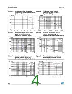
Figure 3.
Peak pulse power dissipation
versus initial junction temperature
(typical values)
Figure 4.
Peak pulse power versus
exponential pulse duration
(T initial = 25 °C)
j
PPP(W)
2000
PPP(kW)
100.0
10.0
1.0
10/1000 µs
1500
1000
500
Tj(°C)
t
(ms)
p
0
0
0.1
25
50
75
100
125
150
175
1.0E-03
1.0E-02
1.0E-01
1.0E+00
1.0E+01
Figure 5.
Clamping voltage versus peak
pulse current (exponential
waveform, maximum values)
Figure 6.
Junction capacitance versus
reverse applied voltage for
unidirectional types (typical values)
IPP(A)
1000.0
C(pF)
10000
Tj initial = 25 °C
F = 1 MHz
VOSC = 30 mVRMS
Tj = 25 °C
SM15T6V8AY
100.0
10.0
1.0
8/20 µs
10/1000 µs
1000
SM15T30AY
SM15T82AY
VCL(V)
1000
VR(V)
1000
0.1
100
1
1
10
100
10
100
Figure 7.
Junction capacitance versus
reverse applied voltage for
bidirectional types (typical values)
Figure 8.
Thermal resistance junction to
ambient versus copper surface
under each lead
C(pF)
10000
Rth(j-a)(°C/W)
100
90
80
70
60
50
40
30
20
10
0
F = 1 MHz
VOSC = 30 mVRMS
Tj = 25 °C
SM15T6V8CAY
Printed circuit board FR4,
copper thickness = 35 µm
SM15T30CAY
1000
SM15T82CAY
SCu(cm²)
4.0 4.5 5.0
VR(V)
1000
100
1
0.0
0.5
1.0
1.5
2.0
2.5
3.0
3.5
10
100
4/12
Doc ID 17865 Rev 3

 STMICROELECTRONICS [ ST ]