Electrical characteristics
STP7NK80Z - STP7NK80ZFP - STB7NK80Z - STB7NK80Z-1
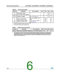
Table 6.
Symbol
Source drain diode
Parameter
Test conditions
Min.
Typ. Max. Unit
ISD
Source-drain current
5.2
A
A
(1)
Source-drain current (pulsed)
20.8
ISDM
(2)
ISD = 5.2 A, VGS = 0
Forward on voltage
1.6
V
VSD
ISD = 5.2 A, di/dt = 100
A/µs
trr
Reverse recovery time
Reverse recovery charge
Reverse recovery current
530
3.31
12.5
ns
Qrr
µC
A
VDD = 50 V, Tj = 150°C
IRRM
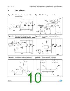
(see Figure 21)
1. Pulsed: pulse duration=300µs, duty cycle 1.5%
2. Pulse width limited by safe operating area
Table 7.
Symbol
Gate-source zener diode
Parameter
Test conditions
Min. Typ. Max. Unit
(1)
BVGSO
Gate-source breakdown voltage Igs= 1mA (Open Drain) 30
V
1. The built-in back-to-back Zener diodes have specifically been designed to enhance not only the device’s
ESD capability, but also to make them safely absorb possible voltage transients that may occasionally be
applied from gate to source. In this respect the Zener voltage is appropriate to achieve an efficient and
cost-effective intervention to protect the device’s integrity. These integrated Zener diodes thus avoid the
usage of external components.
6/18

 STMICROELECTRONICS [ ST ]