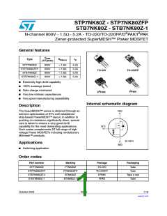
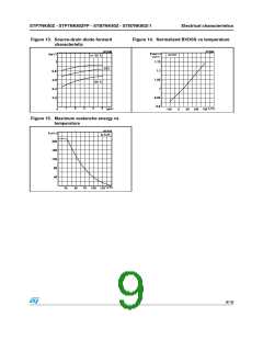
STP7NK80Z - STP7NK80ZFP - STB7NK80Z - STB7NK80Z-1
Electrical characteristics
2
Electrical characteristics
(T
=25°C unless otherwise specified)
CASE
Table 4.
Symbol
On/off states
Parameter
Test conditions
ID =1MA, VGS = 0
Min. Typ. Max. Unit
Drain-source
V(BR)DSS
800
V
Breakdown voltage
VDS = Max rating
Zero gate voltage
1
µA
µA
IDSS
Drain Current (VGS = 0)
VDS = Max rating, TC = 125°C
50
Gate-body leakage
Current (VDS = 0)
IGSS
VGS
=
20 V
10
3.75 4.5
1.5 1.8
µA
VGS(th)
RDS(on)
VDS = VGS, ID = 100 µA
Gate threshold voltage
3
V
Static drain-source on
resistance
VGS = 10 V, ID = 2.6 A
Ω
Table 5.
Symbol
Dynamic
Parameter
Test conditions
Min. Typ. Max. Unit
(1)
VDS = 15v, ID = 2.6 A
Forward transconductance
5
S
gfs
Ciss
Coss
Crss
Input capacitance
Output capacitance
1138
122
25
pF
pF
pF
VDS = 25 V, f = 1 MHz,
VGS = 0
Reverse transfer
capacitance
Coss eq. Equivalent output
VDS =0V, VDS = 0V to 640V
50
pF
capacitance
(2)
td(on)
tr
tr(off)
tr
Turn-on delay time
Rise time
20
12
45
20
ns
ns
ns
ns
VDD = 400 V, ID = 2.6 A,
RG = 4.7 Ω, VGS = 10 V
(see Figure 16)
Turn-off delay time
Fall time
Qg
Qgs
Qgd
VDD = 640 V, ID = 5.2 A,
VGS = 10 V
Total gate charge
Gate-source charge
Gate-drain charge
40
7
56
nC
nC
nC
21
(see Figure 17)
tr(Voff)
VDD = 640 V, ID = 5.2 A,
RG = 4.7 Ω, VGS = 10 V
(see Figure 16)
Off-voltage rise time
Fall time
12
10
20
ns
ns
ns
tr
Cross-over time
tc
1. Pulsed: pulse duration=300µs, duty cycle 1.5%
2. Coss eq. is defined as a constant equivalent capacitance giving the same charging time as Coss when VDS
increases from 0 to 80% VDSS
.
5/18

 STMICROELECTRONICS [ ST ]