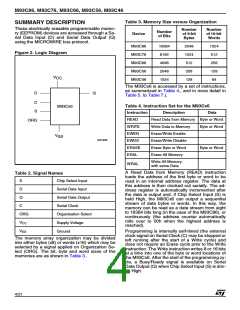
M93C86, M93C76, M93C66, M93C56, M93C46
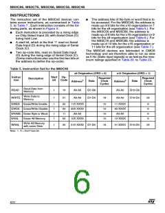
Read
Erase/Write Enable and Disable
The Read Data from Memory (READ) instruction
outputs data on Serial Data Output (Q). When the
instruction is received, the op-code and address
are decoded, and the data from the memory is
transferred to an output shift register. A dummy 0
bit is output first, followed by the 8-bit byte or 16-
bit word, with the most significant bit first. Output
data changes are triggered by the rising edge of
Serial Clock (C). The M93Cx6 automatically incre-
ments the internal address register and clocks out
the next byte (or word) as long as the Chip Select
Input (S) is held High. In this case, the dummy 0 bit
is not output between bytes (or words) and a con-
tinuous stream of data can be read.
The Erase/Write Enable (EWEN) instruction en-
ables the future execution of erase or write instruc-
tions, and the Erase/Write Disable (EWDS)
instruction disables it. When power is first applied,
the M93Cx6 initializes itself so that erase and write
instructions are disabled. After an Erase/Write En-
able (EWEN) instruction has been executed, eras-
ing and writing remains enabled until an Erase/
Write Disable (EWDS) instruction is executed, or
until V
falls below the power-on reset threshold
CC
voltage. To protect the memory contents from ac-
cidental corruption, it is advisable to issue the
Erase/Write Disable (EWDS) instruction after ev-
ery write cycle. The Read Data from Memory
(READ) instruction is not affected by the Erase/
Write Enable (EWEN) or Erase/Write Disable
(EWDS) instructions.
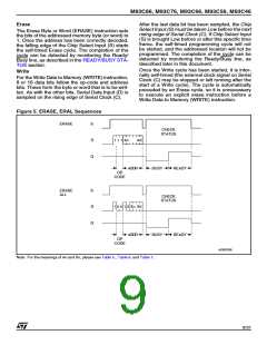
Figure 4. READ, WRITE, EWEN, EWDS Sequences
READ
S
D
Q
1 1 0 An
A0
Qn
Q0
ADDR
DATA OUT
OP
CODE
WRITE
S
D
Q
CHECK
STATUS
1 0 1 An
A0 Dn
D0
ADDR
DATA IN
BUSY
READY
OP
CODE
ERASE
WRITE
ENABLE
S
D
ERASE
WRITE
DISABLE
S
D
1 0 0 1 1 Xn X0
1 0 0 0 0 Xn X0
OP
OP
CODE
CODE
AI00878C
Note: For the meanings of An, Xn, Qn and Dn, see Table 5., Table 6. and Table 7..
8/31

 STMICROELECTRONICS [ ST ]