M93C86, M93C76, M93C66, M93C56, M93C46
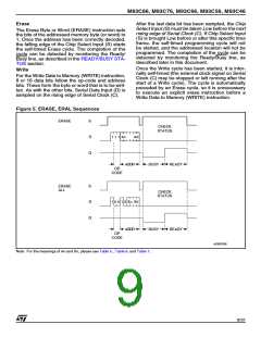
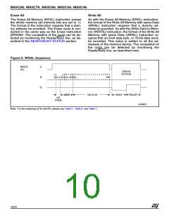
Erase
After the last data bit has been sampled, the Chip
Select Input (S) must be taken Low before the next
rising edge of Serial Clock (C). If Chip Select Input
(S) is brought Low before or after this specific time
frame, the self-timed programming cycle will not
be started, and the addressed location will not be
programmed. The completion of the cycle can be
detected by monitoring the Ready/Busy line, as
described later in this document.
The Erase Byte or Word (ERASE) instruction sets
the bits of the addressed memory byte (or word) to
1. Once the address has been correctly decoded,
the falling edge of the Chip Select Input (S) starts
the self-timed Erase cycle. The completion of the
cycle can be detected by monitoring the Ready/
Busy line, as described in the READY/BUSY STA-
TUS section.
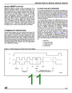
Once the Write cycle has been started, it is inter-
nally self-timed (the external clock signal on Serial
Clock (C) may be stopped or left running after the
start of a Write cycle). The cycle is automatically
preceded by an Erase cycle, so it is unnecessary
to execute an explicit erase instruction before a
Write Data to Memory (WRITE) instruction.
Write
For the Write Data to Memory (WRITE) instruction,
8 or 16 data bits follow the op-code and address
bits. These form the byte or word that is to be writ-
ten. As with the other bits, Serial Data Input (D) is
sampled on the rising edge of Serial Clock (C).
Figure 5. ERASE, ERAL Sequences
ERASE
S
D
Q
CHECK
STATUS
1 1 1 An
A0
ADDR
BUSY
READY
OP
CODE
ERASE
ALL
S
D
Q
CHECK
STATUS
1 0 0 1 0 Xn X0
ADDR
OP
BUSY
READY
CODE
AI00879B
Note: For the meanings of An and Xn, please see Table 5., Table 6. and Table 7..
9/31

 STMICROELECTRONICS [ ST ]