M93C86, M93C76, M93C66, M93C56, M93C46
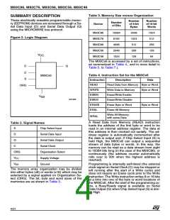
SUMMARY DESCRIPTION
Table 3. Memory Size versus Organization
These electrically erasable programmable memo-
ry (EEPROM) devices are accessed through a Se-
rial Data Input (D) and Serial Data Output (Q)
using the MICROWIRE bus protocol.
Number
of 8-bit
Bytes
Number
of 16-bit
Words
Number
of Bits
Device
M93C86
M93C76
M93C66
M93C56
M93C46
16384
8192
4096
2048
1024
2048
1024
512
1024
512
256
128
64
Figure 2. Logic Diagram
256
V
CC
128
The M93Cx6 is accessed by a set of instructions,
as summarized in Table 4., and in more detail in
Table 5. to Table 7.).
D
Q
C
S
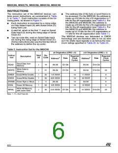
Table 4. Instruction Set for the M93Cx6
M93Cx6
Instruction
READ
Description
Data
Read Data from Memory Byte or Word
ORG
WRITE
EWEN
Write Data to Memory
Erase/Write Enable
Erase/Write Disable
Erase Byte or Word
Erase All Memory
Byte or Word
Byte or Word
V
SS
AI01928
EWDS
ERASE
ERAL
Write All Memory
with same Data
WRAL
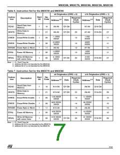
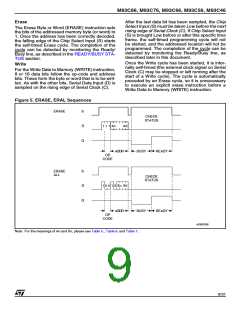
A Read Data from Memory (READ) instruction
loads the address of the first byte or word to be
read in an internal address register. The data at
this address is then clocked out serially. The ad-
dress register is automatically incremented after
the data is output and, if Chip Select Input (S) is
held High, the M93Cx6 can output a sequential
stream of data bytes or words. In this way, the
memory can be read as a data stream from eight
to 16384 bits long (in the case of the M93C86), or
continuously (the address counter automatically
rolls over to 00h when the highest address is
reached).
Table 2. Signal Names
S
Chip Select Input
D
Serial Data Input
Serial Data Output
Serial Clock
Q
C
ORG
Organisation Select
Supply Voltage
Ground
V
CC
V
SS
Programming is internally self-timed (the external
clock signal on Serial Clock (C) may be stopped or
left running after the start of a Write cycle) and
does not require an Erase cycle prior to the Write
instruction. The Write instruction writes 8 or 16 bits
at a time into one of the byte or word locations of
the M93Cx6. After the start of the programming cy-
cle, a Busy/Ready signal is available on Serial
Data Output (Q) when Chip Select Input (S) is driv-
en High.
The memory array organization may be divided
into either bytes (x8) or words (x16) which may be
selected by a signal applied on Organization Se-
lect (ORG). The bit, byte and word sizes of the
memories are as shown in Table 3..
4/31

 STMICROELECTRONICS [ ST ]