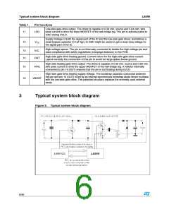
L6599
Electrical characteristics
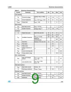
Table 4.
Symbol
Electrical characteristics
Parameter
Test condition
Min
Typ
Max
Unit
Line sensing
Voltage rising or falling
Vth
Threshold voltage
1.2
1.25
15
1.3
V
(1)
IHyst
Current hysteresis
Clamp level
12
6
18
8
µA
V
VCC > 5V, VLINE = 0.3V
ILINE = 1mA
Vclamp
DIS function
IDIS
Vth
VDIS = 0 to Vth
Input bias current
Disable threshold
-1
µA
V
Voltage rising (1)
1.77
1.85
1.93
Oscillator
D
Output duty cycle
Both HVG and LVG
48
50
60
52
%
58.2
240
61.8
260
kHz
RRFmin= 2.7 kΩ
250
fosc
Oscillation frequency
Maximum
recommended
500
0.4
kHz
TD
Dead-time
Peak value
Valley value
Between HVG and LVG
0.2
0.3
3.9
0.9
µs
V
VCFp
VCFv
V
Voltage reference at
pin 4
VREF
(1)
1.92
1
2
1
2.08
100
V
KM
Current mirroring ratio
Timing resistor range
A/A
RFMIN
kΩ
PFC_STOP function
VPFC_STOP = VCC
VDIS = 0V
,
High level leakage
current
Ileak
1
µA
V
IPFC_STOP =1mA,
VDIS = 2V
VL
Low saturation level
0.2
Soft-start function
Ileak
R
Open-state current
V(Css) = 2V
0.5
µA
VISEN > VISENx
Discharge resistance
120
Ω
Standby function
IDIS
Vth
VDIS = 0 to Vth
Input Bias Current
Disable threshold
Hysteresis
-1
µA
V
Voltage falling (1)
Voltage rising
1.2
1.25
50
1.3
Hys
mV
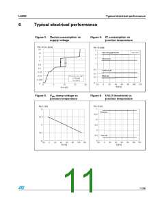
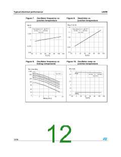
9/36

 STMICROELECTRONICS [ ST ]