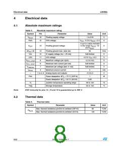
L6599A
Electrical characteristics
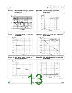
5
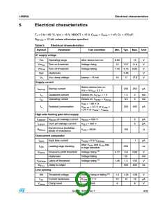
Electrical characteristics
TJ = 0 to 105 °C, Vcc = 15 V, VBOOT = 15 V, CHVG = CLVG = 1 nF; CF = 470 pF;
RRFmin = 12 kΩ; unless otherwise specified.
Table 5.
Symbol
Electrical characteristics
Parameter
Test condition
Min. Typ. Max. Unit
IC supply voltage
Vcc
VccOn
VccOff
Hys
Operating range
After device turn-on
Voltage rising
8.85
10
16
V
V
V
V
V
Turn-on threshold
Turn-off threshold
Hysteresis
10.7
8.15
2.55
17
11.4
8.85
Voltage falling
7.45
VZ
Vcc clamp voltage
Iclamp = 15 mA
16
17.9
Supply current
Before device turn-on
Vcc = VccOn- 0.2 V
Istart-up Startup current
200
250
µA
Iq
Quiescent current
Operating current
Device on, VSTBY = 1 V
Device on, VSTBY = VRFmin
VDIS > 1.85 V or
1.5
3.5
2
5
mA
mA
Iop
Iq
Residual consumption
300
400
µA
VDELAY > 3.5 V or VLINE
1.24 V or VLINE = Vclamp
<
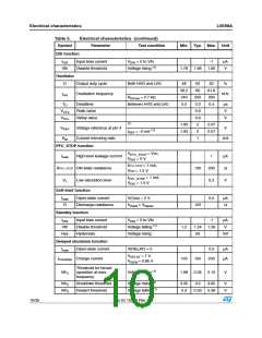
High-side floating gate-drive supply
ILKBOOT VBOOT pin leakage current VBOOT = 580 V
5
5
µA
µA
ILKOUT OUT pin leakage current
VOUT = 562 V
VLVG = HIGH
Synchronous bootstrap
RDS(on)
150
250
Ω
diode on-resistance
Overcurrent comparator
IISEN
tLEB
Input bias current
VISEN = 0 to VISENdis
-1
µA
ns
After VHVG and VLVG low-
to-high transition
Leading edge blanking
VISENx Frequency shift threshold
Hysteresis
Voltage rising (1)
0.77
1.45
0.8
50
0.83
V
mV
V
Voltage falling
VISENdis Latch-off threshold
Voltage rising (1)
1.5
300
1.55
400
td(H-L)
Delay to output
ns
Line sensing
Vth
IHys
Threshold voltage
Voltage rising or falling (1)
VLINE = 1.1 V
1.2
10
6
1.24
13
1.28
16
8
V
µA
V
Current hysteresis
Clamp level
Vclamp
ILINE = 1 mA
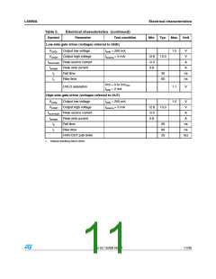
Doc ID 15308 Rev 7
9/35

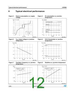
 STMICROELECTRONICS [ ST ]