L6599A
Pin connection
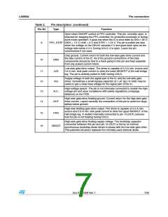
Table 2.
Pin N#
Pin description (continued)
Type
Function
Open-drain ON/OFF control of PFC controller. This pin, normally open, is
intended for stopping the PFC controller, for protection purposes or during
burst mode operation. It goes low when the IC is shut down by DIS>1.85 V,
PFC_STOP ISEN > 1.5 V, LINE > 6 V and STBY < 1.24 V. The pin is pulled low also
when the voltage on the DELAY exceeds 2 V and goes back open as the
voltage falls below 0.3 V. During UVLO, it is open. Leave the pin
unconnected if not used.
9
Chip ground. Current return for both the low-side gate-drive current and
the bias current of the IC. All of the ground connections of the bias
components should be tied to a track going to this pin and kept separate
10
GND
from any pulsed current return.
Low-side gate-drive output. The driver is capable of 0.3 A min. source and
11
12
13
14
LVG
Vcc
0.8 A min. sink peak current to drive the lower MOSFET of the half bridge
leg. The pin is actively pulled to GND during UVLO.
Supply voltage of both the signal part of the IC and the low-side gate
driver. Sometimes a small bypass capacitor (0.1 µF typ.) to GND may be
useful to get a clean bias voltage for the signal part of the IC.
High-voltage spacer. The pin is not internally connected to isolate the high-
voltage pin and ease compliance with safety regulations (creepage
distance) on the PCB.
N.C.
OUT
High-side gate-drive floating ground. Current return for the high-side gate-
drive current. Layout carefully the connection of this pin to avoid too large
spikes below ground.
High-side floating gate-drive output. The driver is capable of 0.3 A min.
source and 0.8 A min. sink peak current to drive the upper MOSFET of the
half bridge leg. A resistor internally connected to pin 14 (OUT) ensures
that the pin is not floating during UVLO.
15
16
HVG
High-side gate-drive floating supply voltage. The bootstrap capacitor
connected between this pin and pin 14 (OUT) is fed by an internal
synchronous bootstrap diode driven in-phase with the low-side gate drive.
This patented structure replaces the normally used external diode.
VBOOT
Doc ID 15308 Rev 7
7/35

 STMICROELECTRONICS [ ST ]