L6599A
Application information
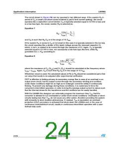
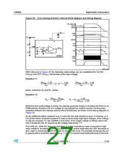
Figure 30. Line sensing function: internal block diagram and timing diagram
(6 )NPUT BUS
/.
6IN
/&&
6IN
T
,).%
ꢁꢅꢂꢇ6
(6 )NPUT BUS
T
T
6CC
6IN/+
ꢁꢂ
)
(93
2(
ꢁꢆ !
,).%
ꢏ
6IN/+
T
ꢊ
ꢁꢆ !
ꢁꢅꢂꢇ6
ꢋ
6CC
ꢊ 6
2,
T
T
,ꢉꢈꢄꢄ!
,6'
(6'
6OUT
T
!-ꢀꢁꢁꢇꢀVꢁ
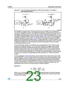
With reference to Figure 28, the following relationships can be established for the ON
(VinON) and OFF (VinOFF) thresholds of the input voltage:
Equation 11
VinON −1.24
VinOFF −1.24
1.24
RL
1.24
RL
= 13 ⋅10−6
+
=
RH
RH
which, solved for RH and RL, yields:
Equation 12
VinON − VinOFF
13 ⋅10−6
1.24
RH
=
;
RL = R
H VinOFF −1.24
While the line undervoltage is active, the startup generator keeps on working but there is no
PWM activity, therefore the Vcc voltage (if not supplied by another source) continuously
oscillates between the startup and the UVLO thresholds, as shown in the timing diagram of
Figure 30.
As an additional safety measure (e.g. in case the low-side resistor is open or missing, or in
non-power factor corrected systems in case of abnormally high input voltage), if the voltage
on the pin exceeds 7 V, the L6599A is shut down. If its supply voltage is always above the
UVLO threshold, the IC restarts as the voltage falls below 7 V.
The LINE pin, while the device is operating, is a high impedance input connected to high
value resistors, therefore it is prone to pick-up noise, which might alter the OFF threshold or
give origin to undesired switch-off of the IC during ESD tests. It is possible to bypass the pin
to ground with a small film capacitor (e.g. 1-10 nF) to prevent any malfunctioning of this kind.
Doc ID 15308 Rev 7
27/35

 STMICROELECTRONICS [ ST ]