Pin settings
L6562A
2
Pin settings
2.1
Pin connection
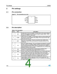
Figure 2. Pin connection (top view)
INV
COMP
MULT
CS
1
2
3
4
8
7
6
5
Vcc
GD
GND
ZCD
2.2
Pin description
Table 2. Pin description
Pin N°
Name
Description
Inverting input of the error amplifier. The information on the output voltage of
the PFC pre-regulator is fed into this pin through a resistor divider. The pin
doubles as an ON/OFF control input.
1
INV
Output of the error amplifier. A compensation network is placed between this
pin and INV to achieve stability of the voltage control loop and ensure high
power factor and low THD.
2
3
COMP
MULT
Main input to the multiplier. This pin is connected to the rectified mains
voltage via a resistor divider and provides the sinusoidal reference to the
current loop.
Input to the PWM comparator. The current flowing in the MOSFET is sensed
through a resistor, the resulting voltage is applied to this pin and compared
with an internal sinusoidal-shaped reference, generated by the multiplier, to
determine MOSFET’s turn-off. The pin is equipped with 200 ns leading-edge
blanking for improved noise immunity.
4
CS
Boost inductor’s demagnetization sensing input for transition-mode
operation. A negative-going edge triggers MOSFET’s turn-on.
5
6
ZCD
GND
Ground. Current return for both the signal part of the IC and the gate driver.
Gate driver output. The totem pole output stage is able to drive power
MOSFET’s and IGBT’s with a peak current of 600 mA source and 800 mA
sink. The high-level voltage of this pin is clamped at about 12V to avoid
excessive gate voltages in case the pin is supplied with a high Vcc.
7
8
GD
Supply Voltage of both the signal part of the IC and the gate driver. The
supply voltage upper limit is extended to 22V min. to provide more headroom
for supply voltage changes.
Vcc
4/26

 STMICROELECTRONICS [ ST ]