8 Mbit / 16 Mbit Multi-Purpose Flash
SST39LF080 / SST39LF016 / SST39VF080 / SST39VF016
Data Sheet
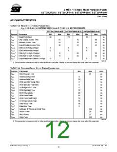
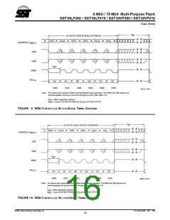
T
BE
SIX-BYTE CODE FOR BLOCK-ERASE
5555 5555 2AAA
5555
2AAA
BA
X
ADDRESS A
MS-0
CE#
OE#
WE#
T
WP
DQ
7-0
AA
55
SW1
80
AA
55
SW4
50
SW0
SW2
SW3
SW5
396 ILL F09.2
Note: The device also supports CE# controlled Block-Erase operation. The WE# and CE# signals are
interchangeable as long as minimum timings are met. (See Table 14)
A
A
= Most significant address
MS
MS
= A for SST39LF/VF080 and A for SST39LF/VF016.
19
20
FIGURE 9: WE# CONTROLLED BLOCK-ERASE TIMING DIAGRAM
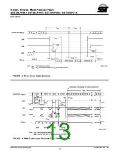
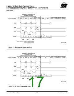
T
SE
SIX-BYTE CODE FOR SECTOR-ERASE
5555
2AAA
5555
5555
2AAA
SA
X
ADDRESS A
MS-0
CE#
OE#
WE#
T
WP
DQ
7-0
AA
55
80
AA
55
30
SW0
SW1
SW2
SW3
SW4
SW5
396 ILL F10.2
Note: The device also supports CE# controlled Sector-Erase operation. The WE# and CE# signals are
interchangeable as long as minimum timings are met. (See Table 14)
A
A
= Most significant address
MS
MS
= A for SST39LF/VF080 and A for SST39LF/VF016.
19
20
FIGURE 10: WE# CONTROLLED SECTOR-ERASE TIMING DIAGRAM
©2001 Silicon Storage Technology, Inc.
S71146-03-000 6/01 396
16

 SST [ SILICON STORAGE TECHNOLOGY, INC ]