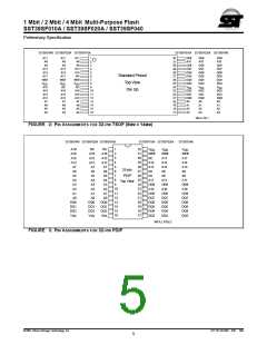
1 Mbit / 2 Mbit / 4 Mbit Multi-Purpose Flash
SST39SF010A / SST39SF020A / SST39SF040
Preliminary Specification
tor- or Chip-Erase, the Data# Polling is valid after the rising
edge of sixth WE# (or CE#) pulse. See Figure 7 for Data#
Polling timing diagram and Figure 16 for a flowchart.
Product Identification
The product identification mode identifies the device as the
SST39SF040, SST39SF010A, or SST39SF020A and
manufacturer as SST. This mode may be accessed by soft-
ware operations. Users may wish to use the software prod-
uct identification operation to identify the part (i.e., using the
device ID) when using multiple manufacturers in the same
socket. For details, see Table 3 for hardware operation or
Table 4 for software operation, Figure 11 for the software ID
entry and read timing diagram and Figure 17 for the ID
entry command sequence flowchart.
Toggle Bit (DQ6)
During the internal Program or Erase operation, any con-
secutive attempts to read DQ6 will produce alternating 0s
and 1s, i.e., toggling between 0 and 1. When the internal
Program or Erase operation is completed, the toggling will
stop. The device is then ready for the next operation. The
Toggle Bit is valid after the rising edge of fourth WE# (or
CE#) pulse for Program operation. For Sector- or Chip-
Erase, the Toggle Bit is valid after the rising edge of sixth
WE# (or CE#) pulse. See Figure 8 for Toggle Bit timing dia-
gram and Figure 16 for a flowchart.
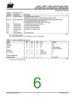
TABLE 1: PRODUCT IDENTIFICATION
Address
Data
Manufacturer’s ID
Device ID
0000H
BFH
Data Protection
SST39SF010A
SST39SF020A
SST39SF040
0001H
0001H
0001H
B5H
B6H
B7H
The SST39SF010A/020A/040 provide both hardware and
software features to protect nonvolatile data from inadvert-
ent writes.
T1.2 398
Hardware Data Protection
Product Identification Mode Exit/Reset
Noise/Glitch Protection: A WE# or CE# pulse of less than 5
ns will not initiate a Write cycle.
In order to return to the standard Read mode, the Software
Product Identification mode must be exited. Exit is accom-
plished by issuing the Exit ID command sequence, which
returns the device to the Read operation. Please note that
the software reset command is ignored during an internal
Program or Erase operation. See Table 4 for software com-
mand codes, Figure 12 for timing waveform and Figure 17
for a flowchart.
VDD Power Up/Down Detection: The Write operation is
inhibited when VDD is less than 2.5V.
Write Inhibit Mode: Forcing OE# low, CE# high, or WE#
high will inhibit the Write operation. This prevents inadvert-
ent writes during power-up or power-down.
Software Data Protection (SDP)
The SST39SF010A/020A/040 provide the JEDEC
approved Software Data Protection scheme for all data
alteration operations, i.e., Program and Erase. Any Pro-
gram operation requires the inclusion of a series of three
byte sequence. The three byte-load sequence is used to
initiate the Program operation, providing optimal protection
from inadvertent Write operations, e.g., during the system
power-up or power-down. Any Erase operation requires the
inclusion of six byte load sequence. The SST39SF010A/
020A/040 devices are shipped with the Software Data Pro-
tection permanently enabled. See Table 4 for the specific
software command codes. During SDP command
sequence, invalid commands will abort the device to read
mode, within TRC
.
©2001 Silicon Storage Technology, Inc.
S71147-02-000 5/01 398
3

 SST [ SILICON STORAGE TECHNOLOGY, INC ]