1 Mbit / 2 Mbit / 4 Mbit Multi-Purpose Flash
SST39SF010A / SST39SF020A / SST39SF040
Preliminary Specification
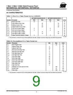
low. The address bus is latched on the falling edge of WE#
or CE#, whichever occurs last. The data bus is latched on
the rising edge of WE# or CE#, whichever occurs first.
Polling or Toggle Bit methods. See Figure 9 for timing
waveforms. Any commands written during the Sector-
Erase operation will be ignored.
Read
Chip-Erase Operation
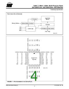
The Read operation of the SST39SF010A/020A/040 is
controlled by CE# and OE#, both have to be low for the
system to obtain data from the outputs. CE# is used for
device selection. When CE# is high, the chip is deselected
and only standby power is consumed. OE# is the output
control and is used to gate data from the output pins. The
data bus is in high impedance state when either CE# or
OE# is high. Refer to the Read cycle timing diagram (Fig-
ure 4) for further details.
The SST39SF010A/020A/040 provide Chip-Erase opera-
tion, which allows the user to erase the entire memory
array to the “1s” state. This is useful when the entire device
must be quickly erased.
The Chip-Erase operation is initiated by executing a six-
byte Software Data Protection command sequence with
Chip-Erase command (10H) with address 5555H in the last
byte sequence. The internal Erase operation begins with
the rising edge of the sixth WE# or CE#, whichever occurs
first. During the internal Erase operation, the only valid read
is Toggle Bit or Data# Polling. See Table 4 for the command
sequence, Figure 10 for timing diagram, and Figure 18 for
the flowchart. Any commands written during the Chip-
Erase operation will be ignored.
Byte-Program Operation
The SST39SF010A/020A/040 are programmed on a byte-
by-byte basis. Before programming, one must ensure that
the sector, in which the byte which is being programmed
exists, is fully erased.The Program operation consists of
three steps. The first step is the three-byte-load sequence
for Software Data Protection. The second step is to load
byte address and byte data. During the Byte-Program
operation, the addresses are latched on the falling edge of
either CE# or WE#, whichever occurs last. The data is
latched on the rising edge of either CE# or WE#, whichever
occurs first. The third step is the internal Program operation
which is initiated after the rising edge of the fourth WE# or
CE#, whichever occurs first. The Program operation, once
initiated, will be completed, within 20 µs. See Figures 5 and
6 for WE# and CE# controlled Program operation timing
diagrams and Figure 15 for flowcharts. During the Program
operation, the only valid reads are Data# Polling and Tog-
gle Bit. During the internal Program operation, the host is
free to perform additional tasks. Any commands written
during the internal Program operation will be ignored.
Write Operation Status Detection
The SST39SF010A/020A/040 provide two software means
to detect the completion of a Write (Program or Erase)
cycle, in order to optimize the system Write cycle time. The
software detection includes two status bits: Data# Polling
(DQ7) and Toggle Bit (DQ6). The End-of-Write detection
mode is enabled after the rising edge of WE# which ini-
tiates the internal Program or Erase operation.
The actual completion of the nonvolatile write is asynchro-
nous with the system; therefore, either a Data# Polling or
Toggle Bit read may be simultaneous with the completion
of the Write cycle. If this occurs, the system may possibly
get an erroneous result, i.e., valid data may appear to con-
flict with either DQ7 or DQ6. In order to prevent spurious
rejection, if an erroneous result occurs, the software routine
should include a loop to read the accessed location an
additional two (2) times. If both reads are valid, then the
device has completed the Write cycle, otherwise the rejec-
tion is valid.
Sector-Erase Operation
The Sector-Erase operation allows the system to erase the
device on a sector-by-sector basis. The sector architecture
is based on uniform sector size of 4 KByte. The Sector-
Erase operation is initiated by executing a six-byte-com-
mand load sequence for Software Data Protection with
Sector-Erase command (30H) and sector address (SA) in
the last bus cycle. The sector address is latched on the fall-
ing edge of the sixth WE# pulse, while the command (30H)
is latched on the rising edge of the sixth WE# pulse. The
internal Erase operation begins after the sixth WE# pulse.
The End-of-Erase can be determined using either Data#
Data# Polling (DQ7)
When the SST39SF010A/020A/040 are in the internal Pro-
gram operation, any attempt to read DQ7 will produce the
complement of the true data. Once the Program operation
is completed, DQ7 will produce true data. The device is
then ready for the next operation. During internal Erase
operation, any attempt to read DQ7 will produce a ‘0’. Once
the internal Erase operation is completed, DQ7 will produce
a ‘1’. The Data# Polling is valid after the rising edge of
fourth WE# (or CE#) pulse for Program operation. For Sec-
©2001 Silicon Storage Technology, Inc.
S71147-02-000 5/01 398
2

 SST [ SILICON STORAGE TECHNOLOGY, INC ]