A d v a n c e I n f o r m a t i o n
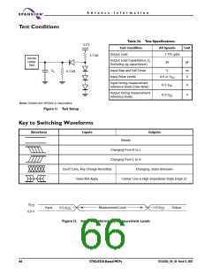
Test Conditions
Table 24. Test Specifications
3.3 V
Test Condition
Output Load
All Speeds
1 TTL gate
Unit
2.7 kΩ
Device
Under
Test
Output Load Capacitance, CL
(including jig capacitance)
30
pF
Input Rise and Fall Times
Input Pulse Levels
5
ns
V
C
L
6.2 kΩ
0.0 or VCC
Input timing measurement
reference levels (See Note)
0.5 VCC
0.5 VCC
V
V
Output timing measurement
reference levels
Note: Diodes are IN3064 or equivalent.
Figure 11. Test Setup
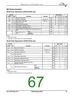
Key to Switching Waveforms
Waveform
Inputs
Outputs
Steady
Changing from H to L
Changing from L to H
Don’t Care, Any Change Permitted
Does Not Apply
Changing, State Unknown
Center Line is High Impedance State (High Z)
V
CC
0.5 V
Input
0.5 V
Measurement Level
Output
CC
CC
0.0 V
Figure 12. Input Waveforms and Measurement Levels
66
S71GL032A Based MCPs
S71GL032A_00_A0 March 31, 2005

 SPANSION [ SPANSION ]