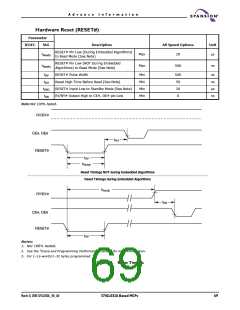
A d v a n c e I n f o r m a t i o n
DC Characteristics
CMOS Compatible
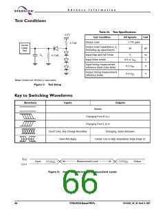
Parameter
Symbol
Parameter Description (Notes)
Test Conditions
Min
Typ
Max
Unit
V
V
IN = VSS to VCC
,
ILI
Input Load Current (Note 1)
A9, ACC Input Load Current
±1.0
µA
CC = VCC max
-40°C to 0°C
0°C to 85°C
250
35
V
CC = VCC max; A9 =
ILIT
µA
12.5 V
ILR
ILO
Reset Leakage Current
Output Leakage Current
VCC = VCC max; RESET# = 12.5 V
35
µA
µA
VOUT = VSS to VCC
,
±1.0
V
CC = VCC max
1 MHz
5
20
25
50
20
40
60
CE# = VIL, OE# =
VIH
ICC1
VCC Initial Read Current (Notes 2, 3)
5 MHz
18
35
5
mA
,
10 MHz
10 MHz
40 MHz
ICC2
VCC Intra-Page Read Current (Notes 2, 3) CE# = VIL, OE# = VIH
mA
10
50
ICC3
ICC4
ICC5
ICC6
VCC Active Write Current (Note 3)
VCC Standby Current (Note 3)
VCC Reset Current (Note 3)
CE# = VIL, OE# = VIH
mA
µA
µA
µA
CE#, RESET# = VCC ± 0.3 V,
WP# = VIH
1
1
1
5
5
5
RESET# = VSS ± 0.3 V, WP# = VIH
V
IH = VCC ± 0.3 V;
Automatic Sleep Mode (Notes 3, 5)
-0.1< VIL ≤ 0.3 V, WP# = VIH
VIL
Input Low Voltage 1 (Note 6)
Input High Voltage 1 (Note 6)
–0.5
0.8
V
V
VIH
0.7 VCC
VCC + 0.5
Voltage for ACC Program
Acceleration
VHH
VCC = 2.7 –3.6 V
VCC = 2.7 –3.6 V
11.5
11.5
12.0
12.0
12.5
V
V
Voltage for Autoselect and Temporary
Sector Unprotect
VID
12.5
0.45
VOL
Output Low Voltage (Note 6)
IOL = 4.0 mA, VCC = VCC min
IOH = –2.0 mA, VCC = VCC min
IOH = –100 µA, VCC = VCC min
V
V
V
V
VOH1
VOH2
VLKO
0.85 VCC
VCC–0.4
2.3
Output High Voltage
Low VCC Lock-Out Voltage (Note 7)
2.5
Notes:
1. On the WP#/ACC pin only, the maximum input load current when WP# = VIL is ± 5.0 µA.
2. The ICC current listed is typically less than 3.5 mA/MHz, with OE# at VIH.
3. Maximum ICC specifications are tested with VCC = VCCmax.
4. ICC active while Embedded Erase or Embedded Program is in progress.
5. Automatic sleep mode enables the low power mode when addresses remain stable for tACC + 30 ns.
6. VCC voltage requirements.
7. Not 100% tested.
March 31, 2005 S71GL032A_00_A0
S71GL032A Based MCPs
65

 SPANSION [ SPANSION ]