P R E L I M I N A R Y
Product Selector Guide
Part Number
S29PL032J/S29PL064J/S29PL127J/S29PL129J
VCC,VIO = 2.7–3.6 V
55 (Note)
60
65
70
VCC = 2.7–3.6 V,
Speed Option
VIO = 1.65–1.95 V (PL127J and
65
70
PL129J only)
Max Access Time, ns (tACC
Max CE# Access, ns (tCE)
)
55 (Note)
20 (Note)
60
25
25
65
25
70
30
70
30
Max Page Access, ns (tPACC
Max OE# Access, ns (tOE)
)
Note: Contact factory for availability
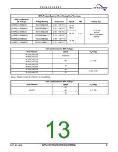
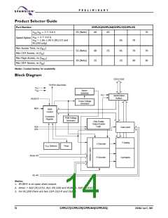
Block Diagram
DQ15–DQ0
RY/BY# (See Note)
V
CC
V
SS
Sector
Switches
V
IO
Input/Output
Buffers
RESET#
WE#
Erase Voltage
Generator
State
Control
Command
Register
PGM Voltage
Generator
Chip Enable
Output Enable
Logic
CE#
OE#
Data Latch
Y-Gating
Y-Decoder
X-Decoder
V
CC
Detector
Timer
Amax–A3
Cell Matrix
A2–A0
Notes:
1. RY/BY# is an open drain output.
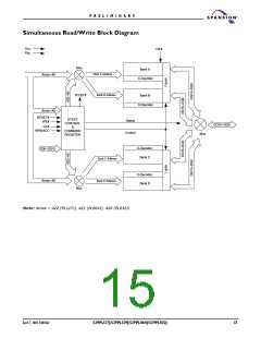
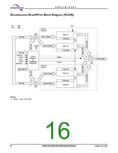
2. Amax = A22 (PL127J), A21 (PL129J and PL064J), A20 (PL032J)
3. For PL129J there are two CE# (CE1# and CE2#)
12
S29PL127J/S29PL129J/S29PL064J/S29PL032J
31107A62 April 7, 2005

 SPANSION [ SPANSION ]