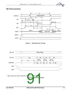
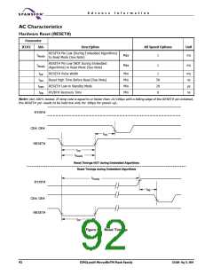
A d v a n c e I n f o r m a t i o n
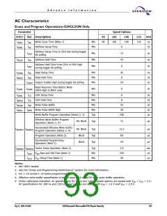
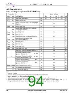
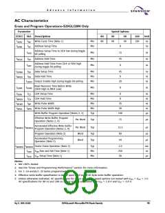
AC Characteristics
Erase and Program Operations–S29GL128N Only
Parameter
Speed Options
JEDEC
tAVAV
Std. Description
tWC Write Cycle Time (Note 1)
tAS
80
90
90
100
Unit
ns
Min
Min
80
90
90
100
tAVWL
Address Setup Time
0
15
45
0
ns
Address Setup Time to OE# low during toggle
bit polling
tASO
tAH
Min
Min
Min
ns
ns
ns
tWLAX
Address Hold Time
Address Hold Time From CE# or OE# high
during toggle bit polling
tAHT
tDVWH
tWHDX
tDS
tDH
Data Setup Time
Data Hold Time
Min
Min
Min
45
0
ns
ns
ns
tOEPH Output Enable High during toggle bit polling
20
Read Recovery Time Before Write
tGHWL
tGHWL
Min
0
ns
(OE# High to WE# Low)
tELWL
tWHEH
tWLWH
tWHDL
tCS
tCH
tWP
CE# Setup Time
CE# Hold Time
Write Pulse Width
Min
Min
Min
Min
Typ
0
0
ns
ns
ns
ns
µs
35
30
240
tWPH Write Pulse Width High
Write Buffer Program Operation (Notes 2, 3)
Effective Write Buffer Program
Per Word
Typ
15
µs
Operation (Notes 2, 4)
Accelerated Effective Write Buffer
Program Operation (Notes 2, 4)
tWHWH1 tWHWH1
Per Word
Word
Typ
Typ
Typ
13.5
60
µs
µs
µs
Program Operation (Note 2)
Accelerated Programming
Operation (Note 2)
Word
54
tWHWH2 tWHWH2 Sector Erase Operation (Note 2)
Typ
Min
Min
1.0
250
50
sec
ns
tVHH
tVCS
VHH Rise and Fall Time (Note 1)
VCC Setup Time (Note 1)
µs
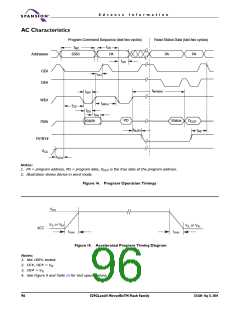
Notes:
1. Not 100% tested.
2. See the “Erase and Programming Performance” section for more information.
3. For 1–16 words/1–32 bytes programmed.
4. Effective write buffer specification is based upon a 16-word/32-byte write buffer operation.
5. Unless otherwise indicated, AC specifications for 80 ns and 90 ns speed options are tested with V = V = 3 V.
IO
CC
AC specifications for 90 ns and 100 ns speed options are tested with V = 1.8 V and V = 3.0 V.
IO
CC
May 13, 2004 27631A4
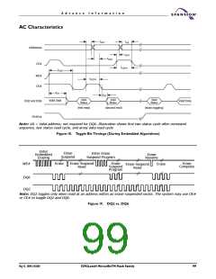
S29GLxxxN MirrorBitTM Flash Family
95

 SPANSION [ SPANSION ]