A d v a n c e I n f o r m a t i o n
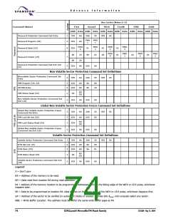
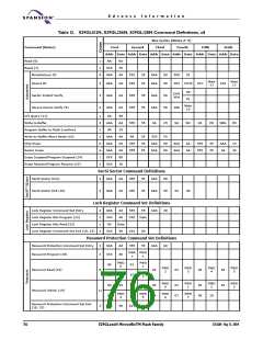
Bus Cycles (Notes 2–5)
Third Fourth
Addr Data Addr Data Addr Data Addr Data Addr Data Addr Data
Command (Notes)
First
Second
Fifth
Sixth
Non-Volatile Sector Protection Command Set Definitions
Nonvolatile Sector Protection Command
Set Entry
3
AAA
AA
55
55
AAA
C0
PPB Program (24, 25)
All PPB Erase
2
2
XXX
XXX
A0
80
SA
00
00
30
RD
(0)
PPB Status Read (25)
1
2
SA
Non-Volatile Sector Protection Command
Set Exit (18)
XXX
90
XXX
00
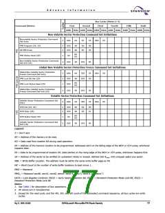
Global Non-Volatile Sector Protection Freeze Command Set Definitions
Global Non-Volatile Sector Protection
Freeze Command Set Entry
3
2
1
AAA
XXX
XXX
AA
A0
555
XXX
55
00
AAA
50
PPB Lock Bit Set (25)
RD
(0)
PPB Lock Status Read (25)
Global Non-Volatile Sector Protection
Freeze Command Set Exit (18)
2
XXX
90
XXX
00
Volatile Sector Protection Command Set Definitions
Volatile Sector Protection Command Set
Entry
3
AAA
AA
555
55
AAA
E0
DYB Set (24, 25)
DYB Clear (25)
2
2
XXX
XXX
A0
A0
SA
SA
00
01
RD
(0)
DYB Status Read (25)
1
2
SA
Volatile Sector Protection Command Set
Exit (18)
XXX
90
XXX
00
Legend:
X = Don’t care
RA = Address of the memory to be read.
RD = Data read from location RA during read operation.
PA = Address of the memory location to be programmed. Addresses latch on the falling edge of the WE# or CE# pulse, whichever
happens later.
PD = Data to be programmed at location PA. Data latches on the rising edge of the WE# or CE# pulse, whichever happens first.
SA = Address of the sector to be verified (in autoselect mode) or erased. Address bits Amax–A16 uniquely select any sector.
WBL = Write Buffer Location. The address must be within the same write buffer page as PA.
WC = Word Count is the number of write buffer locations to load minus 1.
PWD = Password
PWDx = Password word0, word1, word2, word3. word 4, word 5, word 6, and word 7.
DATA = Lock Register Contents: PD(0) = SecSi Sector Protection Bit, PD(1) = Persistent Protection Mode Lock Bit, PD(2) =
Password Protection Mode Lock Bit.
Notes:
1. See Table 1 for description of bus operations.
2. All values are in hexadecimal.
3. Except for the read cycle, and the 4th, 5th, and 6th cycle of the autoselect command sequence, all bus cycles are write
cycles.
May 13, 2004 27631A4
S29GLxxxN MirrorBitTM Flash Family
77

 SPANSION [ SPANSION ]