A d v a n c e I n f o r m a t i o n
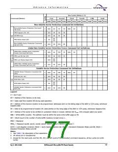
Table 13. S29GL512N, S29GL256N, S29GL128N Command Definitions, x8
Bus Cycles (Notes 2–5)
Command (Notes)
First
Second
Third
Fourth
Fifth
Sixth
Addr Data Addr Data Addr Data Addr Data Addr Data Addr Data
Read (6)
1
1
4
RA
RD
F0
Reset (7)
XXX
AAA
Manufacturer ID
AA
555
555
55
55
AAA
AAA
90
90
X00
X02
01
Note
17
Note
17
Device ID
4
4
4
AAA
AAA
AAA
AA
AA
AA
XX7E
X1C
X1E
00
01
(SA)
X04
Sector Protect Verify
Secure Device Verify (9)
555
555
55
55
AAA
AAA
90
90
Note
10
X06
SA
CFI Query (11)
1
3
1
3
6
6
1
1
AA
98
AA
29
AA
AA
AA
B0
30
Write to Buffer
AAA
SA
555
55
SA
25
WC
PA
PD
WBL
PD
Program Buffer to Flash (confirm)
Write-to-Buffer-Abort Reset (16)
Chip Erase
AAA
AAA
AAA
XXX
XXX
PA
55
55
55
555
AAA
AAA
F0
80
80
555
555
AAA
AAA
AA
AA
555
555
55
55
AAA
SA
10
30
Sector Erase
Erase Suspend/Program Suspend (14)
Erase Resume/Program Resume (15)
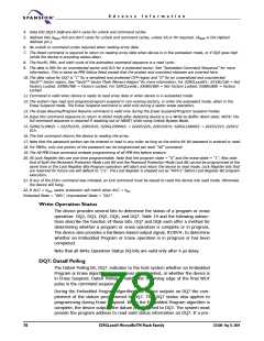
SecSi Sector Command Definitions
SecSi Sector Entry
3
AAA
AA
555
55
AAA
88
SecSi Sector Exit (18)
4
AAA
AA
555
55
AAA
90
XX
00
Lock Register Command Set Definitions
Lock Register Command Set Entry
Lock Register Bits Program (22)
Lock Register Bits Read (22)
3
2
1
2
AAA
XXX
00
AA
A0
555
XXX
55
AAA
40
Data
Data
90
Lock Register Command Set Exit (18, 23)
XXX
XXX
00
Password Protection Command Set Definitions
Password Protection Command Set Entry
3
AAA
AA
555
55
AAA
60
PWA PWD
Password Program (20)
2
XXX
A0
x
x
PWD
0
PWD
1
00
06
01
PWD
2
PWD
3
PWD
4
PWD
5
Password Read (19)
Password Unlock (19)
8
02
03
04
05
03
PWD
6
PWD
7
07
00
PWD
0
PWD
1
PWD
2
PWD
3
00
25
03
00
06
01
07
02
00
11
2
PWD
4
PWD
5
PWD
6
PWD
7
04
05
29
Password Protection Command Set Exit
(18, 23)
XXX
90
XXX
00
76
S29GLxxxN MirrorBitTM Flash Family
27631A4 May 13, 2004

 SPANSION [ SPANSION ]