A d v a n c e I n f o r m a t i o n
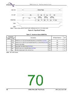
Same Page
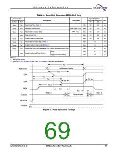
A23-A2
A1-A0*
Ad
Aa
tACC
Ab
tPACC
Ac
tPACC
tPACC
Data Bus
Qa
Qb
Qc
Qd
CE#
OE#
Note: * Figure shows device in word mode. Addresses are A1–A-1 for byte mode
.
Figure 14. Page Read Timings
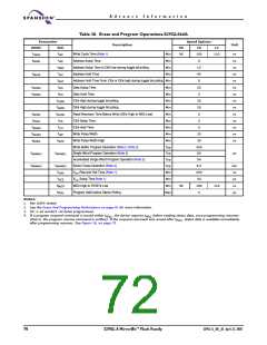
Table 37. Hardware Reset (RESET#)
Parameter
Description
All Speed Options
Unit
JEDEC
Std.
t
t
t
t
t
t
RESET# Pin Low (During Embedded Algorithms) to Read Mode (See Note)
Max
20
500
500
50
µs
ns
ns
ns
µs
ns
Ready
Ready
RP
RESET# Pin Low (NOT During Embedded Algorithms) to Read Mode(See Note) Max
RESET# Pulse Width
Min
Min
Min
Min
Reset High Time Before Read (See Note)
RESET# Input Low to Standby Mode (See Note)
RY/BY# Output High to CE#, OE# pin Low
RH
20
RPD
RB
0
Note: Not 100% tested
.
68
S29GL-A MirrorBit™ Flash Family
S29GL-A_00_A3 April 22, 2005

 SPANSION [ SPANSION ]