A d v a n c e I n f o r m a t i o n
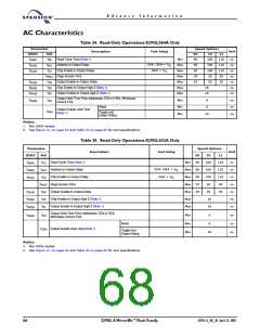
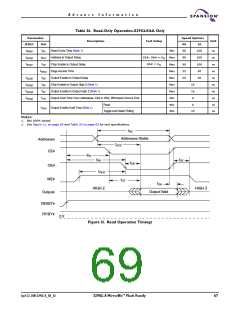
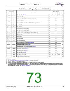
Table 36. Read-Only Operation-S29GL016A Only
Parameter
JEDEC Std.
Speed Options
Description
Test Setup
Unit
90
90
90
90
25
25
10
100
100
100
30
t
t
t
RC
Read Cycle Time (Note 1)
Address to Output Delay
Chip Enable to Output Delay
Page Access Time
Min
Max
Max
Max
Max
Max
Max
ns
ns
ns
ns
ns
ns
ns
AVAV
t
CE#, OE# = V
IL
AVQV
ACC
t
t
OE# = V
IL
ELQV
CE
t
PACC
t
t
t
t
Output Enable to Output Delay
30
GLQV
OE
t
Chip Enable to Output High Z (Note 1)
16
16
EHQZ
DF
t
Output Enable to Output High Z (Note 1)
GHQZ
DF
t
t
Output Hold Time From Addresses, CE# or OE#, Whichever Occurs First
Min
Min
Min
0
0
ns
ns
ns
AXQX
OH
Read
Output Enable Hold Time (Note 1)
Toggle and Data# Polling
t
OEH
10
Notes:
1. Not 100% tested.
2. See Figure 11, on page 65 and Table 33 on page 65 for test specifications.
tRC
Addresses Stable
tACC
Addresses
CE#
tRH
tRH
tDF
tOE
OE#
tOEH
WE#
tCE
tOH
Output Valid
HIGH Z
HIGH Z
Outputs
RESET#
RY/BY#
0 V
Figure 13. Read Operation Timings
April 22, 2005 S29GL-A_00_A3
S29GL-A MirrorBit™ Flash Family
67

 SPANSION [ SPANSION ]