A d v a n c e I n f o r m a t i o n
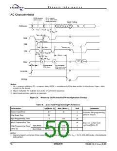
AC Characteristics
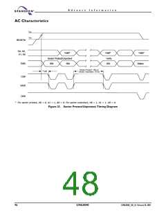
555 for program
PA for program
2AA for erase
SA for sector erase
555 for chip erase
Data# Polling
Addresses
PA
tWC
tWH
tAS
tAH
WE#
OE#
tGHEL
tWHWH1 or 2
tCP
CE#
Data
tWS
tCPH
tDS
tBUSY
tDH
DQ7#
DOUT
tRH
A0 for program
55 for erase
PD for program
30 for sector erase
10 for chip erase
RESET#
RY/BY#
Notes:
1. PA = program address, PD = program data, DQ7# = complement of the data written to the device, DOUT = data
written to the device.
2. Figure indicates the last two bus cycles of command sequence.
3. Word mode address used as an example.
Figure 24. Alternate CE# Controlled Write Operation Timings
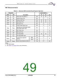
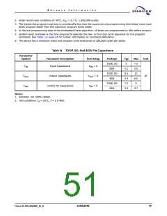
Table 15. Erase And Programming Performance
Parameter
Typ (Note 1)
Max (Note 2)
Unit
s
Comments
Sector Erase Time
Chip Erase Time
0.7
11
5
10
Excludes 00h programming
prior to erasure
s
Byte Programming Time
Word Programming Time
150
210
12.5
8.5
µs
µs
s
7
Excludes system level
overhead (Note 5)
Byte Mode
Word Mode
4.2
2.9
Chip Programming Time
(Note 3)
s
Notes:
1. Typical program and erase times assume the following conditions: 25°C, VCC = 3.0 V, 100,000 cycles, checkerboard
data pattern.
48
S29AL004D
S29AL004D_00_A1 February 18, 2005

 SPANSION [ SPANSION ]