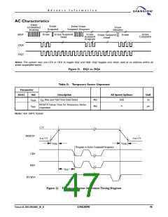
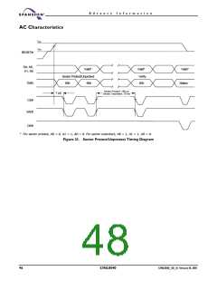
A d v a n c e I n f o r m a t i o n
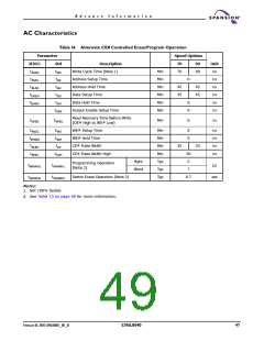
2. Under worst case conditions of 90°C, VCC = 2.7 V, 1,000,000 cycles.
3. The typical chip programming time is considerably less than the maximum chip programming time listed, since most
bytes program faster than the maximum program times listed.
4. In the pre-programming step of the Embedded Erase algorithm, all bytes are programmed to 00h before erasure.
5. System-level overhead is the time required to execute the two- or four-bus-cycle sequence for the program
command. See Table on page 24 for further information on command definitions.
6. The device has a minimum erase and program cycle endurance of 100,000 cycles per sector
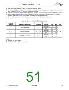
Table 16. TSOP, SO, And BGA Pin Capacitance
Parameter
Symbol
Parameter Description
Test Setup
Package
TSOP, SO
BGA
Typ
6
Max
7.5
5.0
12
Unit
CIN
Input Capacitance
VIN = 0
4.2
8.5
5.4
7.5
3.9
TSOP, SO
BGA
COUT
Output Capacitance
VOUT = 0
VIN = 0
pF
6.5
9
TSOP, SO
BGA
CIN2
Control Pin Capacitance
4.7
Notes:
1. Sampled, not 100% tested.
2. Test conditions TA = 25°C, f = 1.0 MHz.
February 18, 2005 S29AL004D_00_A1
S29AL004D
49

 SPANSION [ SPANSION ]