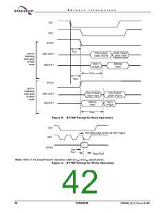
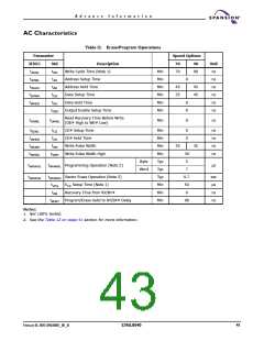
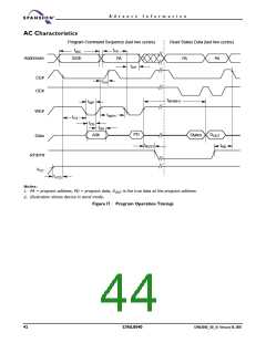
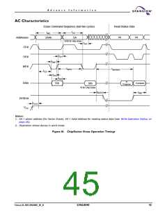
PDF
最近搜索
热门搜索
发布采购

| 型号: | S29AL004D70MFI013 |
| PDF下载: | 下载PDF文件 查看货源 |
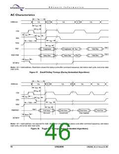
| 内容描述: | 4兆位( 512 Kx的8位/ 256千×16位) CMOS 3.0伏只引导扇区闪存 [4 Megabit (512 Kx 8-Bit/256 K x 16-Bit) CMOS 3.0 Volt-only Boot Sector Flash Memory] |
| 分类和应用: | 闪存 |
| 文件页数/大小: | 55 页 / 1488 K |
| 品牌: |  SPANSION [ SPANSION ] SPANSION [ SPANSION ] |
专业IC领域供求交易平台:提供全面的IC Datasheet资料和资讯,Datasheet 1000万数据,IC品牌1000多家。