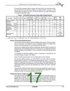
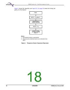
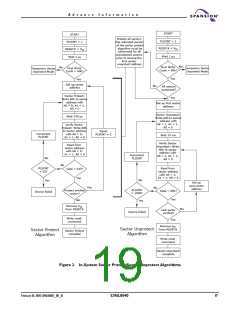
A d v a n c e I n f o r m a t i o n
is in the standby mode, but the standby current is greater. The device requires
standard access time (t ) for read access when the device is in either of these
CE
standby modes, before it is ready to read data.
If the device is deselected during erasure or programming, the device draws ac-
tive current until the operation is completed.
In the iDC Characteristics table, I
specification.
and I
represents the standby current
CC4
CC3
Automatic Sleep Mode
The automatic sleep mode minimizes Flash device energy consumption. The de-
vice automatically enables this mode when addresses remain stable for t + 30
ACC
ns. The automatic sleep mode is independent of the CE#, WE#, and OE# control
signals. Standard address access timings provide new data when addresses are
changed. While in sleep mode, output data is latched and always available to the
system. I
in the iDC Characteristics table represents the automatic sleep mode
CC4
current specification.
RESET#: Hardware Reset Pin
The RESET# pin provides a hardware method of resetting the device to reading
array data. When the RESET# pin is driven low for at least a period of t , the
RP
device immediately terminates any operation in progress, tristates all output
pins, and ignores all read/write commands for the duration of the RESET# pulse.
The device also resets the internal state machine to reading array data. The op-
eration that was interrupted should be reinitiated once the device is ready to
accept another command sequence, to ensure data integrity.
Current is reduced for the duration of the RESET# pulse. When RESET# is held
at V ±0.3 V, the device draws CMOS standby current (I
). If RESET# is held
SS
CC4
at V but not within V ±0.3 V, the standby current is greater.
IL
SS
The RESET# pin may be tied to the system reset circuitry. A system reset would
thus also reset the Flash memory, enabling the system to read the boot-up firm-
ware from the Flash memory.
If RESET# is asserted during a program or erase operation, the RY/BY# pin re-
mains a 0 (busy) until the internal reset operation is complete, which requires a
time of t
(during Embedded Algorithms). The system can thus monitor RY/
READY
BY# to determine whether the reset operation is complete. If RESET# is asserted
when a program or erase operation is not executing (RY/BY# pin is 1), the reset
operation is completed within a time of t
(not during Embedded Algorithms).
READY
The system can read data t
after the RESET# pin returns to V .
IH
RH
Refer to the tables AC Characteristics‚ on page 37 for RESET# parameters and
to Figure 14, on page 38 for the timing diagram.
Output Disable Mode
When the OE# input is at V , output from the device is disabled. The output pins
IH
are placed in the high impedance state.
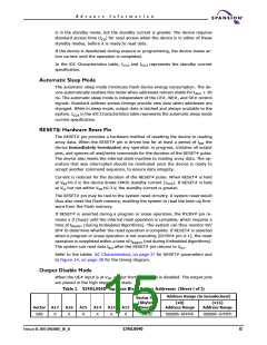
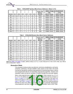
Table 2. S29AL004D Top Boot Block Sector Addresses (Sheet 1 of 2)
Address Range (in hexadecimal)
Sector Size
(Kbytes/
Kwords)
(x8)
(x16)
Sector
A17
A16
A15
A14
A13
A12
Address Range
Address Range
SA0
0
0
0
X
X
X
64/32
00000h–0FFFFh
00000h–07FFFh
February 18, 2005 S29AL004D_00_A1
S29AL004D
13

 SPANSION [ SPANSION ]