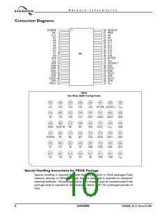
A d v a n c e I n f o r m a t i o n
content occurs during the power transition. No command is necessary in this
mode to obtain array data. Standard microprocessor read cycles that assert valid
addresses on the device address inputs produce valid data on the device data
outputs. The device remains enabled for read access until the command register
contents are altered.
See Reading Array Data‚ on page 18 for more information. Refer to the AC table
for timing specifications and to Figure 13, on page 37 for the timing diagram. I
CC1
in the DC Characteristics table represents the active current specification for
reading array data.
Writing Commands/Command Sequences
To write a command or command sequence (which includes programming data
to the device and erasing sectors of memory), the system must drive WE# and
CE# to V , and OE# to V .
IL
IH
For program operations, the BYTE# pin determines whether the device accepts
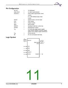
program data in bytes or words. Refer to Word/Byte Configuration‚ on page 11
for more information.
The device features an Unlock Bypass mode to facilitate faster programming.
Once the device enters the Unlock Bypass mode, only two write cycles are re-
quired to program a word or byte, instead of four. The Word/Byte Program
Command Sequence‚ on page 19 has details on programming data to the device
using both standard and Unlock Bypass command sequences.
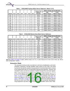
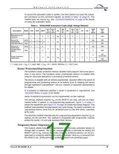
An erase operation can erase one sector, multiple sectors, or the entire device.
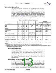
Table 2 on page 13 and Table on page 14 indicate the address space that each
sector occupies. A sector address consists of the address bits required to uniquely
select a sector. The Command Definitions‚ on page 18 has details on erasing a
sector or the entire chip, or suspending/resuming the erase operation.
After the system writes the autoselect command sequence, the device enters the
autoselect mode. The system can then read autoselect codes from the internal
register (which is separate from the memory array) on DQ7–DQ0. Standard read
cycle timings apply in this mode. Refer to the Autoselect Mode‚ on page 14 and
Autoselect Command Sequence‚ on page 19 for more information.
I
in the DC Characteristics table represents the active current specification for
CC2
the write mode. The AC Characteristics‚ on page 37 contains timing specification
tables and timing diagrams for write operations.
Program and Erase Operation Status
During an erase or program operation, the system may check the status of the
operation by reading the status bits on DQ7–DQ0. Standard read cycle timings
and I read specifications apply. Refer to Write Operation Status‚ on page 26 for
CC
more information, and to AC Characteristics‚ on page 37 for timing diagrams.
Standby Mode
When the system is not reading or writing to the device, it can place the device
in the standby mode. In this mode, current consumption is greatly reduced, and
the outputs are placed in the high impedance state, independent of the OE#
input.
The device enters the CMOS standby mode when the CE# and RESET# pins are
both held at V
0.3 V. (Note that this is a more restricted voltage range than
CC
V .) If CE# and RESET# are held at V , but not within V
CC
0.3 V, the device
S29AL004D_00_A1 February 18, 2005
IH
IH
12
S29AL004D

 SPANSION [ SPANSION ]