Highly Integrated Full Featured Hi-Speed USB 2.0 ULPI Transceiver
Datasheet
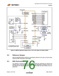
VDDIO Supply
Link Controller
14
11
8
REFSEL2
REFSEL1
REFSEL0
27
RESETB
RESETB
13
10
9
7
6
5
4
3
29
2
DATA7
DATA6
DATA5
DATA4
DATA3
DATA2
DATA1
DATA0
STP
DATA7
DATA6
DATA5
DATA4
DATA3
DATA2
DATA1
DATA0
STP
17
CPEN
RVBUS must be
installed to enable
overvoltage
protection of the
VBUS pin.
VBUS
Switch
EN
RVBUS
NXT
NXT
31
1
5V
22
DIR
DIR
IN OUT
VBUS
CLKOUT
CLKIN
3.1-5.5V
Supply
25
26
The capacitor CVBUS
must be installed on
XO
Resonator
- or -
21
20
this side of RVBUS
.
VBAT
1MΩ
CBYP
VDD33
REFCLK
USB
CVBUS
COUT
Receptacle
Crystal
and Caps
VBUS
ID
CLOAD
23
19
18
ID
VDDIO Supply
32
DM
DM
DP
VDDIO
VDD18
1.8V Supply
DP
CBYP
28, 30
SHIELD
GND
CBYP
15
16
SPK_L
SPK_R
24
RBIAS
GND
RBIAS
For Host applications (non-OTG), the
ID pin should be connected to GND.
Optional
Switched Signal
to DP/DM
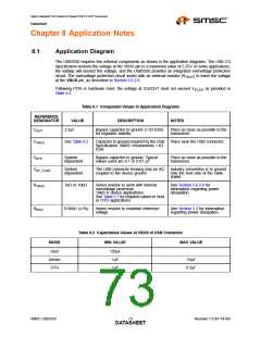
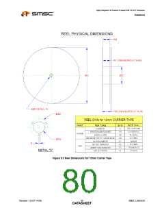
Figure 8.3 USB3320 Application Diagram (Host or OTG, ULPI Output Clock Mode, 24MHz)
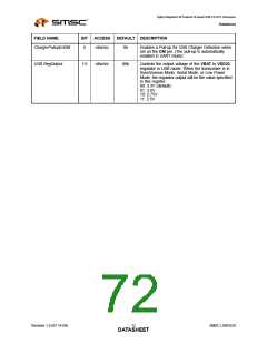
8.2
8.3
Reference Designs
SMSC has generated reference designs for connecting the USB3320 to SOCs with a ULPI port. Please
contact the SMSC sales office for more details.
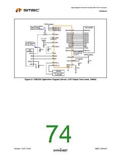
ESD Performance
The USB3320 is protected from ESD strikes. By eliminating the requirement for external ESD
protection devices, board space is conserved, and the board manufacturer is enabled to reduce cost.
The advanced ESD structures integrated into the USB3320 protect the device whether or not it is
powered up.
Revision 1.0 (07-14-09)
SMSC USB3320
DATA7S6HEET

 SMSC [ SMSC CORPORATION ]