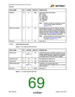
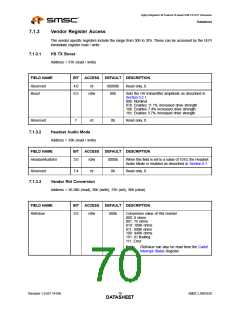
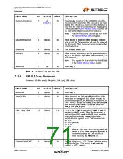
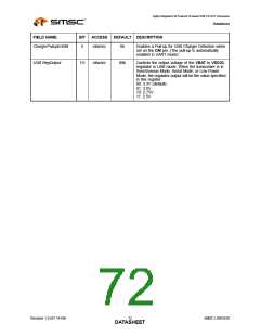
Highly Integrated Full Featured Hi-Speed USB 2.0 ULPI Transceiver
Datasheet
Chapter 8 Application Notes
8.1
Application Diagram
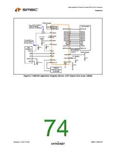
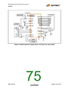
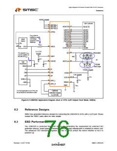
The USB3320 requires few external components as shown in the application diagrams. The USB 2.0
Specification restricts the voltage at the VBUS pin to a maximum value of 5.25V. In some applications,
the voltage will exceed this voltage, and the USB3320 provides an integrated overvoltage protection
circuit. The overvoltage protection circuit works with an external resistor (RVBUS) to lower the voltage
at the VBUS pin, as described in Section 5.6.2.6.
Following POR or hardware reset, the voltage at CLKOUT must not exceed VIH_ED as provided in
Table 4.4.
Table 8.1 Component Values in Application Diagrams
REFERENCE
DESIGNATOR
VALUE
2.2μF
DESCRIPTION
NOTES
COUT
Bypass capacitor to ground (<1Ω ESR)
for regulator stability.
Place as close as possible to the
transceiver.
CVBUS
See Table 8.2
Capacitor to ground required by the USB
Specification. SMSC recommends <1Ω
ESR.
Place near the USB connector.
CBYP
System
dependent.
Bypass capacitor to ground. Typical
values used are 0.1 or 0.01 μF.
Place as close as possible to the
transceiver.
CDC_LOAD
System
dependent.
The USB connector housing may be AC- Industry convention is to ground
coupled to the device ground.
only the host side of the cable
shield.
RVBUS
1kΩ or 10kΩ
8.06kΩ (±1%)
Series resistor to work with internal
overvoltage protection.
10kΩ in device applications.
See Table 5.7 for required values in Host
or OTG applications.
See Section 5.6.2.6 for
information regarding power
dissipation.
RBIAS
Series resistor to establish reference
voltage.
See Section 5.3 for information
regarding power dissipation.
Table 8.2 Capacitance Values at VBUS of USB Connector
MODE
MIN VALUE
MAX VALUE
Host
Device
OTG
120μF
1μF
10μF
1μF
6.5μF
SMSC USB3320
Revision 1.0 (07-14-09)
DATA7S3HEET

 SMSC [ SMSC CORPORATION ]