USB 2.0 High-Speed 4-Port Hub Controller
Datasheet
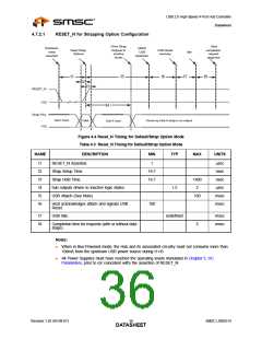
4.3.2.1
4.3.2.2
Implementation Characteristics
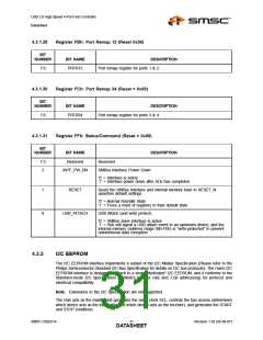
The Hub will only access an EEPROM using the Sequential Read Protocol.
Pull-Up Resistor
The Circuit board designer is required to place external pull-up resistors (10KΩ recommended) on the
SDA/SMBDATA & SCL/SMBCLK/CFG_SELO lines (per SMBus 1.0 Specification, and EEPROM
manufacturer guidelines) to Vcc in order to assure proper operation.
4.3.2.3
I2C EEPROM Slave Address
Slave address is 1010000.
Note: 10-bit addressing is NOT supported.
4.3.3
In-Circuit EEPROM Programming
The EEPROM can be programmed via ATE by pulling RESET_N low (which tri-states the Hub’s
EEPROM interface and allows an external source to program the EEPROM).
4.4
SMBus Slave Interface
Instead of loading User-Defined Descriptor data from an external EEPROM, the SMSC Hub can be
configured to receive a code load from an external processor via an SMBus interface. The SMBus
interface shares the same pins as the EEPROM interface; if CFG_SEL1 & CFG_SEL0 activates the
SMBus interface, external EEPROM support is no longer available (and the user-defined descriptor
data must be downloaded via the SMBus). Due to system issues, the SMSC Hub waits indefinitely for
the SMBus code load to complete and only “appears” as a newly connected device on USB after the
code load is complete.
The Hub’s SMBus implementation is a subset of the SMBus interface to the host. The device is a
slave-only SMBus device. The implementation in the device is a subset of SMBus since it only supports
two protocols.
The Write Block and Read Block protocols are the only valid SMBus protocols for the Hub. The Hub
responds to other protocols as described in Section 4.4.2, "Invalid Protocol Response Behavior," on
page 33. Reference the System Management Bus Specification, Rev 1.0.
The SMBus interface is used to read and write the registers in the device. The register set is shown
in Section 4.3.1, "Internal Register Set (Common to EEPROM and SMBus)," on page 19.
4.4.1
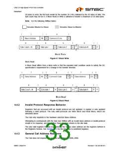
Bus Protocols
Typical Write Block and Read Block protocols are shown below. Register accesses are performed
using 7-bit slave addressing, an 8-bit register address field, and an 8-bit data field. The shading
indicates the Hub driving data on the SMBDATA line; otherwise, host data is on the SDA/SMBDATA
line.
The slave address is the unique SMBus Interface Address for the Hub that identifies it on SMBus. The
register address field is the internal address of the register to be accessed. The register data field is
the data that the host is attempting to write to the register or the contents of the register that the host
is attempting to read.
Note: Data bytes are transferred MSB first (msb first).
4.4.1.1
Block Read/Write
The Block Write begins with a slave address and a write condition. After the command code, the host
issues a byte count which describes how many more bytes will follow in the message. If a slave had
Revision 1.92 (05-08-07)
SMSC USB2514
DATA3S2HEET

 SMSC [ SMSC CORPORATION ]