USB 2.0 High-Speed 4-Port Hub Controller
Datasheet
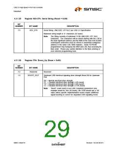
4.3.1.27
Register F8h: Boost_4:0 (Reset = 0x00)
BIT NAME
BIT
NUMBER
DESCRIPTION
7:6
BOOST_IOUT_4
Upstream USB electrical signaling drive strength Boost Bit for Downstream
Port ‘4’.
‘00’ = Normal electrical drive strength
‘01’ = Elevated electrical drive strength (+4% boost)
‘10’ = Elevated electrical drive strength (+8% boost)
‘11’ = Elevated electrical drive strength (+12% boost)
5:4
BOOST_IOUT_3
Upstream USB electrical signaling drive strength Boost Bit for Downstream
Port ‘3’.
‘00’ = Normal electrical drive strength
‘01’ = Elevated electrical drive strength (+4% boost)
‘10’ = Elevated electrical drive strength (+8% boost)
‘11’ = Elevated electrical drive strength (+12% boost)
Note:
“Boost” could result in non-USB Compliant parameters (one
example would be Test J/K levels), the OEM should use a ‘00’
value unless specific implementation issues require additional
signal boosting to correct for degraded USB signalling levels.
3:2
BOOST_IOUT_2
Upstream USB electrical signaling drive strength Boost Bit for Downstream
Port ‘2’.
‘00’ = Normal electrical drive strength
‘01’ = Elevated electrical drive strength (+4% boost)
‘10’ = Elevated electrical drive strength (+8% boost)
‘11’ = Elevated electrical drive strength (+12% boost)
Note:
“Boost” could result in non-USB Compliant parameters (one
example would be Test J/K levels), the OEM should use a ‘00’
value unless specific implementation issues require additional
signal boosting to correct for degraded USB signalling levels.
1:0
BOOST_IOUT_1
Upstream USB electrical signaling drive strength Boost Bit for Downstream
Port ‘1’.
‘00’ = Normal electrical drive strength
‘01’ = Elevated electrical drive strength (+4% boost)
‘10’ = Elevated electrical drive strength (+8% boost)
‘11’ = Elevated electrical drive strength (+12% boost)
Note:
“Boost” could result in non-USB Compliant parameters (one
example would be Test J/K levels), the OEM should use a ‘00’
value unless specific implementation issues require additional
signal boosting to correct for degraded USB signalling levels.
4.3.1.28
Register FAh: Port Swap (Reset = 0x00)
BIT NAME
BIT
NUMBER
DESCRIPTION
7:0
PRTSP
Port Swap: Swaps the Upstream and Downstream USB DP and DM Pins for
ease of board routing to devices and connectors.
‘0’ = USB D+ functionality is associated with the DP pin and D- functionality
is associated with the DM pin.
‘1’ = USB D+ functionality is associated with the DM pin and D- functionality
is associated with the DP pin.
Revision 1.92 (05-08-07)
SMSC USB2514
DATA3S0HEET

 SMSC [ SMSC CORPORATION ]