2
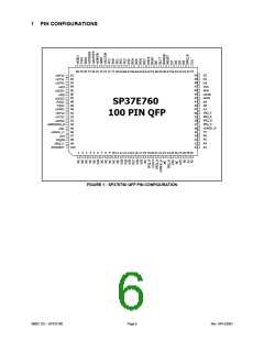
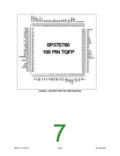
PIN DESCRIPTION
2.1 Buffer Type Per Pin
Table 1 - DESCRIPTION OF PIN FUNCTIONS
PIN #
BUFFER
NAME
SYMBOL
DESCRIPTION
TYPE
TQFP
QFP
HOST PROCESSOR INTERFACE
46-49
51-54
48-51
53-56
Data Bus 0-7 D0-D7
IO12
The data bus connection used by the host
microprocessor to transmit data to and from the chip.
These pins are in a high-impedance state when not in
the output mode.
42
43
44
44
45
46
nI/O Read
nI/O Write
nIOR
nIOW
AEN
IS
IS
IS
This active low signal is issued by the host micropro-
cessor to indicate an I/O read operation.
This active low signal is issued by the host micropro-
cessor to indicate an I/O write operation.
Active high Address Enable indicates DMA operations
on the host data bus. Used internally to qualify
appropriate address decodes.
Address
Enable
26-32
39-41,
95
28-34
41-43,
97
Address Bus A0-A10
I
These host address bits determine the I/O address to
be accessed during nIOR and nIOW cycles. These
bits are latched internally by the leading edge of nIOR
and nIOW. All internal address decodes use the full
A0 to A10 address bits.
19,50,
97
21,52,
99
DMA Request DRQ_A
O12
These active high outputs are the DMA request for
byte transfers of data between the host and the chip.
These signals are cleared on the last byte of the data
transfer by the nDACK signal going low (or by nIOR
going low if nDACK was already low as in demand
mode).
These are active low inputs acknowledging the
request for a DMA transfer of data between the host
and the chip. These inputs enable the DMA read or
write internally.
This signal indicates that DMA data transfer is
complete. TC is only accepted when nDACK_x is
low. In AT and PS/2 model 30 modes, TC is active
high and in PS/2 mode, TC is active low.
A, B, C
nDMA
DRQ_B
DRQ_C
20,34,
94
22,36,
96
nDACK_A
IS
IS
Acknowl-edge nDACK_B
A, B, C
nDACK_C
33
35
Terminal
Count
TC
17,
19,
37-40, 24
Interrupt
Request
IRQ_A
IRQ_C
IRQ_D
IRQ_E
IRQ_F
IRQ_H
nCS
O12/OD12 Interrupt requests from a logical device or IRQIN are
output on one of the IRQA-H signals. Refer to the
configuration registers section for additional
information.
35-38, 22
A, C, D,
E, F, and H
If EPP or ECP Mode is enabled this output is pulsed
low and released to allow sharing of interrupts.
25
55
27
57
Chip Select
Input
I
This active low input serves as an external decoder
for address lines above A10.
This active high signal resets the chip and must be
valid for 500ns minimum. The effect on the internal
registers is described in the appropriate section. The
configuration registers are not affected by this reset.
Reset
RESET
IS
98
86
100
88
I/O Channel
IOCHRDY
OD12
This pin is pulled low to extend the read/write
command. IOCHRDY can be used by the Parallel
Port in EPP mode.
Ready (Note3)
SERIAL PORTS INTERFACE
Receive Data RXD2
IS
Receiver serial data input for port 2.
2
SMSC DS – SP37E760
Page 8
Rev. 04/13/2001

 SMSC [ SMSC CORPORATION ]