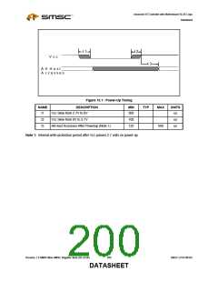
Advanced I/O Controller with Motherboard GLUE Logic
Datasheet
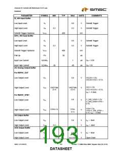
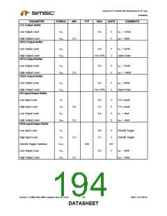
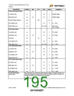
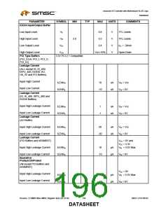
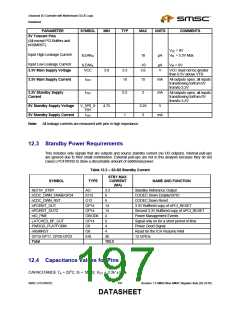
PARAMETER
5V Tolerant Pins
SYMBOL
MIN
TYP
MAX
UNITS
COMMENTS
(All except PCI Buffers and
nRSMRST)
V
CC = 0V
Input High Leakage Current
ILEAKIH
10
µA
VIN = 5.5V Max
Input Low Leakage Current
3.3V Main Supply Voltage
ILEAKIL
VCC
-10
3.6
µA
V
VIN = 0V
3.0
3.3
10
VCC must not be greater
than 0.5V above VTR
3.3V Main Supply Current
ICC3
15
mA
All outputs open, all inputs
transitioning to/from 0V
from/to 3.3V
3.3V Standby Supply
Current
ITR3
0.2
2
mA
All outputs open, all inputs
transitioning to/from 0V
from/to 3.3V
5V Standby Supply Voltage
5V Standby Supply Current
V_5P0_S
TBY
4.75
5.25
3
V
ITR5
1
mA
Note: All leakage currents are measured with pins in high impedance.
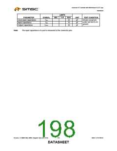
12.3 Standby Power Requirements
This includes only signals that are outputs and source standby current (no OD outputs). Internal pull-ups
are ignored due to their small contribution. External pull-ups are not in this analysis because they do not
cause LPC47M182 to draw a discernable amount of additional power.
Table 12.2 – S3-S5 Standby Current
STBY MAX.
SYMBOL
REF5V_STBY
TYPE
CURRENT
NAME AND FUNCTION
(MA)
AO
3.3
Standby Reference Output
nCDC_DWN_ENAB/GP24
nCDC_DWN_RST
nPCIRST_OUT
nPCIRST_OUT2
nIO_PME
LATCHED_BF_CUT
PWRGD_PLATFORM
nRSMRST
GP10-GP17, GP20-GP23
Total
IO12
O12
6
6
14
14
4
0
4
4
CODEC Down Enable/GPIO
CODEC Down Reset
OP14
OP14
O8/OD8
OP14
O8
3.3V Buffered copy of nPCI_RESET
Second 3.3V Buffered copy of nPCI_RESET
Power Management Events
Signal only on for a short period of time
Power Good Signal
O8
IO8
Reset for the ICH Resume Well
12 GPIOs
48
103.3
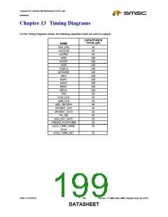
12.4 Capacitance Values for Pins
CAPACITANCE TA = 25oC; fc = 1MHz; VCC = 3.3V ±10%
SMSC LPC47M182
197
Revision 1.8 SMSC/Non-SMSC Register Sets (02-24-05)
DATASHEET

 SMSC [ SMSC CORPORATION ]