Advanced I/O Controller with Motherboard GLUE Logic
Datasheet
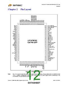
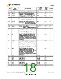
Chapter 3 Description of Pin Functions
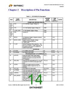
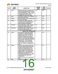
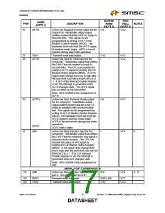
Table 3.1 - LPC47M182 Pin Description
BUFFER
PWR
WELL
NAME
PIN#
DESCRIPTION
NAME
NOTES
(NOTE 1)
(NOTE 2)
(NOTE 3)
POWER AND GROUND PINS (20)
6,31,
49,60,
123
VCC
+3.3 Volt Main Supply Voltage (5)
PWR
76,93, VTR
+3.3 Volt Standby Supply Voltage (4)
PWR
107
71
V_5P0_STBY
VSS
+5 Volt Standby Supply Voltage.
Ground (7)
PWR
PWR
8,29,
46,58,
78,96,
110
70
REF5V
5V Reference Output. Requires external
pull-up to VCC5V.
Highest System Standby Voltage.
Requires external pull-up to
V_5P0_STBY.
AO
AO
VCC
VTR
72
REF5V_STBY
97
F_CAP
Internal Regulator Filter Capacitor. This
pin is a no connect. A filter capacitor can
be placed on this pin if it is required by
system board layout.
CLOCKS (2)
14.318Mhz Clock Input
32.768kHz Clock Input
65
91
CLOCKI
CLOCKI32
IS
IS
VCC
VTR
4
5
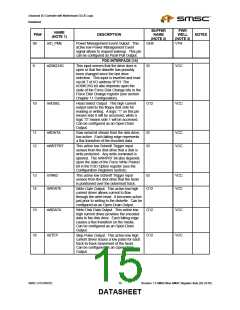
PROCESSOR/HOST LPC INTERFACE (11)
52
nLPCPD
Active low input Power Down signal
indicates that the LPC47M182 should
prepare for power to be shut-off on the
LPC interface.
PCI_I
VCC
53
54
SER_IRQ
nLDRQ
Serial IRQ pin used with the PCI_CLK pin PCI_IO
to transfer LPC47M182 interrupts to the
host.
VCC
VCC
Active low output used for encoded
DMA/Bus Master request for the LPC
interface.
PCI_O
55
56
PCI_CLK
nLFRAME
33.33 MHz PCI Clock input.
PCI_ICLK
PCI_I
VCC
VCC
Active low input indicates start of new
cycle and termination of broken cycle.
Active high LPC I/O used for multiplexed
command, address and data bus.
PCI_IO
PCI_I
VCC
VCC
Active low input used as LPC Interface
Reset. 3.3V and 5V buffered copy of PCI
Reset signal is available on
nPCIRST_OUT and nIDE_RSTDRV.
These pins are listed under GLUE PINS.
Revision 1.8 SMSC/Non-SMSC Register Sets (02-24-05)
14
SMSC LPC47M182
DATASHEET

 SMSC [ SMSC CORPORATION ]