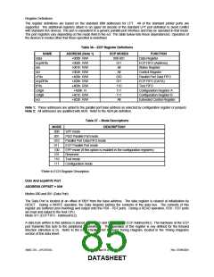
Device Status Register (DSR)
ADDRESS OFFSET = 01H
The Status Port is located at an offset of '01H' from the base address. Bits 0 - 2 are not implemented as register bits,
during a read of the Printer Status Register these bits are a low level. The bits of the Status Port are defined as follows:
BIT 3 nFault
The level on the nFault input is read by the CPU as bit 3 of the Device Status Register.
BIT 4 Select
The level on the Select input is read by the CPU as bit 4 of the Device Status Register.
BIT 5 PError
The level on the PError input is read by the CPU as bit 5 of the Device Status Register. Printer Status Register.
BIT 6 nAck
The level on the nAck input is read by the CPU as bit 6 of the Device Status Register.
BIT 7 nBusy
The complement of the level on the BUSY input is read by the CPU as bit 7 of the Device Status Register.
Device Control Register (DCR)
ADDRESS OFFSET = 02H
The Control Register is located at an offset of '02H' from the base address. The Control Register is initialized to zero by
the RESET input, bits 0 to 5 only being affected; bits 6 and 7 are hard wired low.
BIT 0 STROBE - STROBE
This bit is inverted and output onto the nSTROBE output.
BIT 1 AUTOFD - AUTOFEED
This bit is inverted and output onto the nAUTOFD output. A logic 1 causes the printer to generate a line feed after each
line is printed. A logic 0 means no autofeed.
BIT 2 nINIT - nINITIATE OUTPUT
This bit is output onto the nINIT output without inversion.
BIT 3 SELECTIN
This bit is inverted and output onto the nSLCTIN output. A logic 1 on this bit selects the printer; a logic 0 means the
printer is not selected.
BIT 4 ackIntEn - INTERRUPT REQUEST ENABLE
The interrupt request enable bit when set to a high level may be used to enable interrupt requests from the Parallel
Port to the CPU due to a low to high transition on the nACK input. Refer to the description of the interrupt under
Operation, Interrupts.
BIT 5 DIRECTION
If mode=000 or mode=010, this bit has no effect and the direction is always out regardless of the state of this bit. In all
other modes, Direction is valid and a logic 0 means that the printer port is in output mode (write); a logic 1 means that
the printer port is in input mode (read).
BITS 6 and 7 during a read are a low level, and cannot be written.
cFifo (Parallel Port Data FIFO)
ADDRESS OFFSET = 400h
Mode = 010
Bytes written or DMAed from the system to this FIFO are transmitted by a hardware handshake to the peripheral using
the standard parallel port protocol. Transfers to the FIFO are byte aligned. This mode is only defined for the forward
direction.
SMSC DS – LPC47S45x
Page 86 of 259
Rev. 07/09/2001
DATASHEET

 SMSC [ SMSC CORPORATION ]