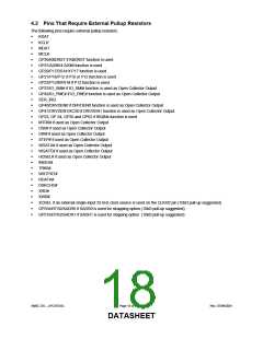
GPIOs for wakeup. See below.
Note: The Fan Tachometer can generate a PME when VCC=0. Clear the enable bits for the fan tachometer before
removing fan power.
The following apply to all I/O pins that are specified to be 5 volt tolerant:
I/O buffers that are wake-up event compatible are powered by VCC. Under VTR power (VCC=0), these pins
may only be configured as inputs. These pins have input buffers into the wakeup logic that are powered by VTR.
I/O buffers that may be configured as either push-pull or open drain under VTR power (VCC=0), are powered by
VTR. This means at a minimum, they will source their specified current from VTR even when VCC is present.
The GPIOs that are used for PME wakeup inputs are GP10-GP17, GP20-GP27, GP30-GP37, GP41, GP43, GP50-
GP57, GP60, GP61. These GPIOs function as follows (with the exception of GP53, GP60 and GP61 - see below):
Buffers are powered by VCC, but in the absence of VCC they are backdrive protected (they do not impose a load
on any external VTR powered circuitry). They are wakeup compatible as inputs under VTR power. These pins
have input buffers into the wakeup logic that are powered by VTR.
All GPIOs listed above are for PME wakeup as a GPIO function (or alternate function). Note that GP33 cannot be
used for wakeup under VTR power (VCC=0) since this is the fan control pin which comes up as output and low
following a VCC POR and PCI Reset. GP53 cannot be used for wakeup under VTR power since this has the IRTX
function and comes up as output and low following a VTR POR, a VCC POR and PCI Reset. Also, GP33 reverts to is
non-inverting GPIO input function when VCC is removed from the part. GP43 reverts to the basic GPIO function
when VCC is removed from the part, but its programmed input/output, invert/non-invert output buffer type is retained.
The other GPIOs function as follows:
GP40, GP62:
Buffers powered by VCC, but in the absence of VCC they are backdrive protected. These pins do not have input
buffers into the wakeup logic that are powered by VTR.
These pins are not used for wakeup:
GP42, GP53, GP60, GP61:
Buffers powered by VTR.
GP42 is the IO_PME# pin.
GP53 has IRTX as the alternate function and its output buffer is powered by VTR so that the pin is always forced
low on VTR POR, VCC POR and PCI Reset. The IRTX pin (GP53/TXD2/IRTX) is powered by VTR so that it are
driven low when VCC = 0V with VTR = 3.3V. This pin is driven low on VTR POR, VCC POR and PCI Reset
regardless of the selected pin function and regardless of the state of internal PWRGOOD (i.e., when VCC=3.3V
and when VCC=0V with VTR=3.3V). The GP53/TXD2/IRTX pin will remain low following a VCC POR until the
serial port is enabled by setting the activate bit, at which time the pin will reflect the state of the IR transmit output
of the IRCC block. If the TXD2 function is selected for the pin, it will remain low following a VCC POR until the
serial port is enabled by setting the activate bit, at which time the pin will reflect the state of the transmit output of
the serial port. If the GPIO output function is selected, the pin will reflect the state of the data bit.
GP60 and GP61 are used for the LED functions.
See the Table in the GPIO section for more information.
The following list summarizes the blocks, registers and pins that are powered by VTR:
PME interface block
•
Runtime register block (includes all PME, SMI, GPIO and other miscellaneous registers)
Configuration Registers
“Wake on Specific Key” logic
LED control logic
Pins for PME Wakeup:
-
GP42/IO_PME# (output, buffer powered by VTR)
SMSC DS – LPC47S45x
Page 22 of 259
Rev. 07/09/2001
DATASHEET

 SMSC [ SMSC CORPORATION ]