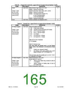
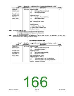
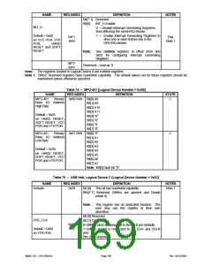
NAME
REG INDEX
DEFINITION
NOTES
Bit[7:1] Reserved
Bit[0]
INT_G Enable
INT_G
0 = Disable Interrupt Generating Registers
from affecting the serial IRQ stream.
Default = 0x00
1 = Enable Interrupt Generating Registers to
drive one or more frames low in the
SER IRQ stream
0xF1
R/W
Eng.
Note 1
on VCC POR, VTR
POR,
HARD
RESET and SOFT
RESET
Note:
See runtime registers at offset 0x54 and
0x55 for configuring Interrupt Generating
Registers.
0xF2-
0xFF
Reserved – read as ‘0’
Note: The registers located in Logical Device A are runtime registers.
Note 1: SMSC Reserved registers have read/write capability. The default values set for these registers should be
maintained unless otherwise specified.
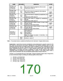
Table 74 – MPU-401 [Logical Device Number = 0x0B]
NAME
REG INDEX
DEFINITION
STATE
MPU-401
Primary 0x60 R/W Bit[0] A8
C
Base I/O Address
High Byte
Bit[1] A9
Bit[2] A10
Bit[3] A11
Bit[4] “0”
Bit[5] “0”
Bit[6] “0”
Bit[7] “0”
Default = 0x03
on HARD RESET,
SOFT RESET, VCC
POR and VTR POR
MPU-401
Primary 0x61 R/W Bit[0] “0”
C
Base I/O Address
Low Byte
Bit[1] A1
Bit[2] A2
Bit[3] A3
Bit[4] A4
Bit[5] A5
Bit[6] A6
Bit[7] A7
Default = 0x30
on HARD RESET,
SOFT RESET, VCC
POR and VTR POR
Note: Bit[0] must be “0”.
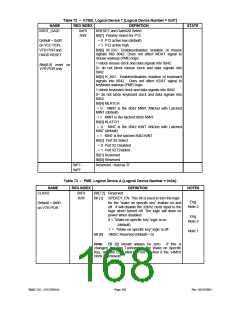
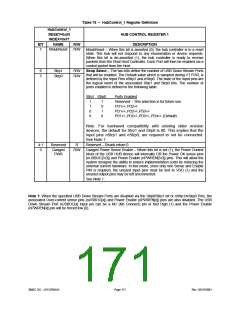
Table 75 – USB Hub, Logical Device C [Logical Device Number = 0x0C]
NAME
Activate
REG INDEX
DEFINITION
This bit has read/write capability.
Bits[7:1] Reserved (Writes are ignored and Reads
NOTES
Note 1
0x30
Bit [0]
return 0)
Note: This register has no dedicated function. The
user may use this register at their own
discretion.
Bit [0] Reserved
OSC_CLK
Bit [1] OSC_CLK
0xF0
R/W
0=48MHz clock is connected to the ICLK pin (default)
Default = 0x00
on VTR POR
1=24MHz crystal is connected to the ICLK and OCLK
pins
Bits [7:2] Reserved
SMSC DS – LPC47M14X
Page 169
Rev. 03/19/2001

 SMSC [ SMSC CORPORATION ]