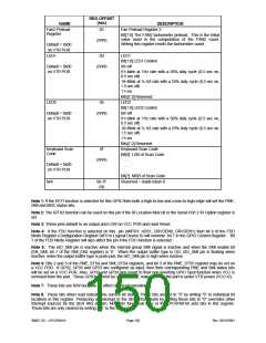
REG OFFSET
(hex)
NAME
DESCRIPTION
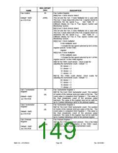
Fan Preload Register 2
Bit[7:0] The FAN2 tachometer preload. This is the initial
value used in the computation of the FAN2 count.
Writing this register resets the tachometer count.
Fan2 Preload
5C
Register
(R/W)
Default = 0x00
on VTR POR
LED1
5D
LED1
Bit[1:0] LED1 Control
00=off
Default = 0x00
on VTR POR
(R/W)
01=blink at 1Hz rate with a 50% duty cycle (0.5 sec on,
0.5 sec off)
10=Blink at ½ HZ rate with a 25% duty cycle (0.5 sec on,
1.5 sec off)
11=on
Bits[7:2] Reserved
LED2
LED2
5E
Bit[1:0] LED2 Control
00=off
Default = 0x00
on VTR POR
(R/W)
01=blink at 1Hz rate with a 50% duty cycle (0.5 sec on,
0.5 sec off)
10=Blink at ½ HZ rate with a 25% duty cycle (0.5 sec on,
1.5 sec off)
11=on
Bits[7:2] Reserved
Keyboard Scan Code
Bit[0] LSB of Scan Code
. . .
Keyboard Scan
Code
5F
(R/W)
Default = 0x00
on VTR POR
. . .
. . .
Bit[7] MSB of Scan Code
Reserved – reads return 0
N/A
60-7F
(R)
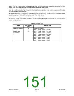
Note 1: If the EETI function is selected for this GPIO then both a high-to-low and a low-to-high edge will set the PME,
SMI and MSC status bits.
Note 2: The IRTX2 function can be used on this pin if the IR Location Mux bit in the Serial Port 2 IR Option register is
set.
Note 3: These pins default to an output and LOW on VCC POR and Hard Reset.
Note 4: If the FDC function is selected on this pin (nMTR1, nDS1, DRVDEN0, DRVDEN1) then bit 6 of the FDD
Mode Register (Configuration Register 0xF0 in Logical Device 0) will override bit 7 in the GPIO Control Register. Bit
7 of the FDD Mode Register will also affect the pin if the FDC function is selected.
Note 5: The nIO_SMI pin is inactive when the internal group SMI signal is inactive and when the SMI enable bit
(EN_SMI, bit 7 of the SMI_EN2 register) is ‘0’. When the output buffer type is OD, nIO_SMI pin is floating when
inactive; when the output buffer type is push-pull, the nIO_SMI pin is high when inactive.
Note 6: Bits 2 and 3 of the PME_STS4 and SMI_STS4 registers, and bit 3 of the PME_STS5 register may be set on
a VCC POR. If GP32, GP33 and GP53 are configured as input, then their corresponding PME and SMI status bits
will be set on a VCC POR. Also, GP32 and GP33 pins revert to their non-inverting GPIO input function when VCC is
removed from the part. These GPIOs cannot be used for PME wakeup when the part is under VTR power (VCC=0).
Note 7: These bits are R/W but have no effect on circuit operation.
Note 8: These bits when read indicate the current bit status. These bits are set to “0” by writing “0” to individual bit
locations in this register. Producing an interrupt in the SER IRQ stream by setting these bits to “0” overrides other
interrupt sources for the SER IRQ stream. No other functional logic in the LPC47M14X sets bits in this register.
These bits are only cleared by writing a ‘1’ to the bit location.
SMSC DS – LPC47M14X
Page 150
Rev. 03/19/2001

 SMSC [ SMSC CORPORATION ]