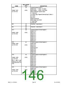
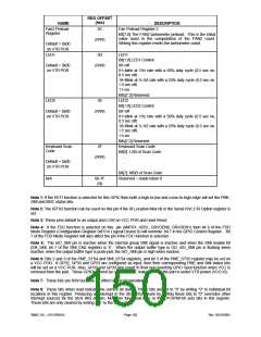
REG OFFSET
(hex)
NAME
DESCRIPTION
General Purpose I/0 bit 6.1
GP61
48
Bit[0] In/Out : =1 Input, =0 Output
Bit[1] Polarity : =1 Invert, =0 No Invert
Bit[3:2] Alternate Function Select
11=Reserved
Default = 0x01
on VTR POR
(R/W)
10=Either Edge Triggered Interrupt Input 5 (Note 1)
01=LED2
00=GPIO
Bits[6:4] Reserved
Bit[7] Output Type Select
1=Open Drain
0=Push Pull
Reserved – reads return 0
N/A
N/A
GP1
49
(R)
4A
(R)
4B
Reserved – reads return 0
General Purpose I/0 Data Register 1
Bit[0] GP10
Default = 0x00
on VTR POR
(R/W)
Bit[1] GP11
Bit[2] GP12
Bit[3] GP13
Bit[4] GP14
Bit[5] GP15
Bit[6] GP16
Bit[7] GP17
GP2
Default = 0x00
on VTR POR
4C
General Purpose I/0 Data Register 2
Bit[0] GP20
(R/W)
Bit[1] GP21
Bit[2] GP22
Bit[3] Reserved
Bit[4] GP24
Bit[5] GP25
Bit[6] GP26
Bit[7] GP27
GP3
4D
General Purpose I/0 Data Register 3
Bit[0] GP30
Default = 0x00
on VTR POR
(R/W)
Bit[1] GP31
Bit[2] GP32
Bits
2
and
3
are
Bit[3] GP33
reset on VCC POR,
Hard Reset and VTR
POR
Bit[4] GP34
Bit[5] GP35
Bit[6] GP36
Bit[7] GP37
GP4
4E
General Purpose I/0 Data Register 4
Bit[0] GP40
Default = 0x00
on VTR POR
(R/W)
Bit[1] GP41
Bit[2] GP42
Bit[3] GP43
Bit[7:4] Reserved
SMSC DS – LPC47M14X
Page 146
Rev. 03/19/2001

 SMSC [ SMSC CORPORATION ]