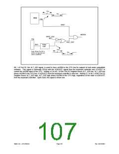
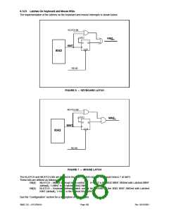
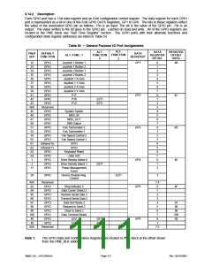
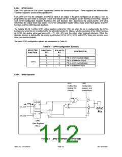
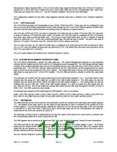
6.14.2 Description
Each GPIO port has a 1-bit data register and an 8-bit configuration control register. The data register for each GPIO
port is represented as a bit in one of the 8-bit GPIO DATA Registers, GP1 to GP6. The bits in these registers reflect
the value of the associated GPIO pin as follows. Pin is an input: The bit is the value of the GPIO pin. Pin is an
output: The value written to the bit goes to the GPIO pin. Latched on read and write. All of the GPIO registers are
located in the PME block see “Run Time Register” section. The GPIO ports with their alternate functions and
configuration state register addresses are listed in Table 54.
Table 54 – General Purpose I/O Port Assignments
ALT.
ALT.
FUNCTION
2
DATA
REGISTER
BIT NO.
REGISTER
OFFSET
(HEX)
PIN #
QFP
DEFAULT
DATA
FUNCTION
ALT. FUNC. 1
FUNCTION
REGISTER1
3
32
33
34
35
36
37
38
39
41
42
43
N/A
45
46
47
50
51
52
54
55
61
62
63
64
1
GPIO
GPIO
GPIO
GPIO
GPIO
GPIO
GPIO
GPIO
GPIO
GPIO
GPIO
Reserved
GPIO
GPIO
GPIO
GPIO
GPIO
GPIO
GPIO
GPIO
Infrared Rx
Infrared Tx
GPIO
GPIO
GPIO
GPIO
GPIO
Joystick 1 Button 1
Joystick 1 Button 2
Joystick 2 Button 1
Joystick 2 Button 2
Joystick 1 X-Axis
Joystick 1 Y-Axis
Joystick 2 X-Axis
Joystick 2 Y-Axis
P17
GP1
GP2
GP3
0
1
2
3
4
5
6
7
0
1
2
3
4
5
6
7
0
1
2
3
4
5
6
7
0
1
2
4B
4C
4D
P16
P12
EETI
EETI
System Option
MIDI_IN
MIDI_OUT
SMI Output
Fan Tachometer 2
Fan Tachometer 1
Fan Speed Control 2
Fan Speed Control 1
GPIO
GPIO
Keyboard Reset
Gate A20
Drive Density Select 0
Drive Density Select 1
GP4
GP5
4E
4F
2
17
EETI
Power Management
Event
28
GPIO
Device Disable Reg.
Control
EETI
3
N/A
92
94
95
96
97
98
99
100
48
Reserved
GPIO
GPIO
GPIO
GPIO
GPIO
GPIO
GPIO
GPIO
7:4
0
1
2
3
4
5
6
7
Ring Indicator 2
Data Carrier Detect 2
Receive Serial Data 2
Transmit Serial Data 2
Data Set Ready 2
Request to Send 2
Clear to Send 2
Date Terminal Ready
LED
97
98
99
100
50
GPIO
GPIO
EETI
EETI
GP6
0
1
49
LED
N/A
Reserved
7:2
Note 1:
The GPIO Data and Configuration Registers are located in PME block at the offset shown
from the PME_BLK address.
SMSC DS – LPC47M14X
Page 111
Rev. 03/19/2001

 SMSC [ SMSC CORPORATION ]