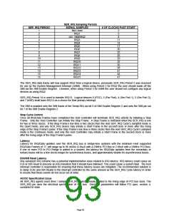
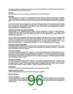
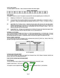
Host I/F Status Register
The Status register is 8 bits wide. Table 53 shows the contents of the Status register.
Table 53 - Status Register
D7
D6
D5
D4
D3
D2
D1
D0
UD
UD
UD
UD
C/D
UD
IBF
OBF
Status Register
This register is cleared on a reset. This register is read-only for the Host and read/write by the LPC47M10x CPU.
UD
Writable by LPC47M10x CPU. These bits are user-definable.
C/D
(Command Data)-This bit specifies whether the input data register contains data or a command (0 = data, 1 =
command). During a host data/command write operation, this bit is set to "1" if SA2 = 1 or reset to "0" if SA2 =
0.
IBF
(Input Buffer Full)- This flag is set to 1 whenever the host system writes data into the input data register.
Setting this flag activates the LPC47M10x CPU's nIBF (MIRQ) interrupt if enabled. When the LPC47M10x CPU
reads the input data register (DBB), this bit is automatically reset and the interrupt is cleared. There is no
output pin associated with this internal signal.
OBF
(Output Buffer Full) - This flag is set to whenever the LPC47M10x CPU write to the output data register (DBB).
When the host system reads the output data register, this bit is automatically reset.
EXTERNAL CLOCK SIGNAL
The LPC47M10x Keyboard Controller clock source is a 12 MHz clock generated from a 14.318 MHz clock. The reset
pulse must last for at least 24 16 MHz clock periods. The pulse-width requirement applies to both internally (Vcc POR)
and externally generated reset signals. In powerdown mode, the external clock signal is not loaded by the chip.
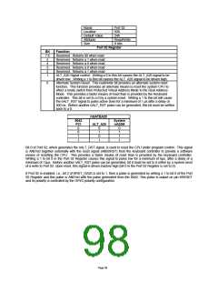
DEFAULT RESET CONDITIONS
The LPC47M10x has one source of hardware reset: an external reset via the nPCI_RESET pin. Refer to Table 46 for
the effect of each type of reset on the internal registers.
Table 54 - Resets
HARDWARE RESET
DESCRIPTION
(nPCI_RESET)
KCLK
KDAT
MCLK
MDAT
Host I/F Data Reg
Host I/F Status Reg
Low
Low
Low
Low
N/A
00H
N/A: Not Applicable
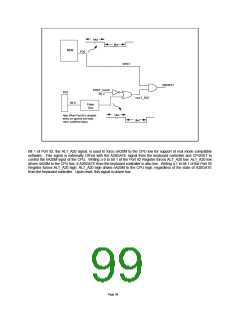
GATEA20 AND KEYBOARD RESET
The LPC47M10x provides two options for GateA20 and Keyboard Reset: 8042 Software Generated GateA20 and
KRESET and Port 92 Fast GateA20 and KRESET.
PORT 92 FAST GATEA20 AND KEYBOARD RESET
Port 92 Register
This port can only be read or written if Port 92 has been enabled via bit 2 of the KRST_GA20.
Register (Logical Device 7, 0xF0) set to 1.
This register is used to support the alternate reset (nALT_RST) and alternate A20 (ALT_A20) functions.
Page 97

 SMSC [ SMSC CORPORATION ]