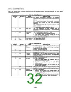
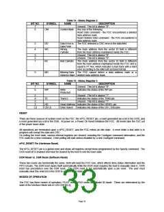
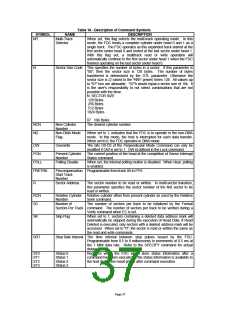
Table 14 - Status Register 2
NAME
BIT NO.
SYMBOL
CM
DESCRIPTION
Unused. This bit is always "0".
Control Mark Any one of the following:
Read Data command - the FDC encountered a deleted
7
6
data address mark.
Read Deleted Data command - the FDC encountered a
data address mark.
5
4
DD
Data Error in
Data Field
Wrong
The FDC detected a CRC error in the data field.
WC
The track address from the sector ID field is different
from the track address maintained inside the FDC.
Unused. This bit is always "0".
Cylinder
3
2
1
Unused. This bit is always "0".
BC
Bad Cylinder The track address from the sector ID field is different
from the track address maintained inside the FDC and is
equal to FF hex, which indicates a bad track with a hard
error according to the IBM soft-sectored format.
0
MD
Missing Data The FDC cannot detect a data address mark or a
Address Mark deleted data address mark.
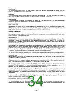
Table 15 - Status Register 3
BIT NO.
SYMBOL
NAME
DESCRIPTION
Unused. This bit is always "0".
Indicates the status of the WP pin.
7
6
WP
T0
Write
Protected
Track 0
5
4
3
Unused. This bit is always "1".
Indicates the status of the TRK0 pin.
Unused. This bit is always "1".
2
1,0
HD
DS1,0
Head Address Indicates the status of the HDSEL pin.
Drive Select Indicates the status of the DS1, DS0 pins.
RESET
There are three sources of system reset on the FDC: the nPCI_RESET pin, a reset generated via a bit in the DOR, and
a reset generated via a bit in the DSR. At power on, a Power On Reset initializes the FDC. All resets take the FDC out
of the power down state.
All operations are terminated upon a nPCI_RESET, and the FDC enters an idle state. A reset while a disk write is in
progress will corrupt the data and CRC.
On exiting the reset state, various internal registers are cleared, including the Configure command information, and the
FDC waits for a new command. Drive polling will start unless disabled by a new Configure command.
nPCI_RESET Pin (Hardware Reset)
The nPCI_RESET pin is a global reset and clears all registers except those programmed by the Specify command. The
DOR reset bit is enabled and must be cleared by the host to exit the reset state.
DOR Reset vs. DSR Reset (Software Reset)
These two resets are functionally the same. Both will reset the FDC core, which affects drive status information and the
FIFO circuits. The DSR reset clears itself automatically while the DOR reset requires the host to manually clear it. DOR
reset has precedence over the DSR reset. The DOR reset is set automatically upon a pin reset. The user must
manually clear this reset bit in the DOR to exit the reset state.
MODES OF OPERATION
The FDC has three modes of operation, PC/AT mode, PS/2 mode and Model 30 mode. These are determined by the
state of the Interface Mode bits in LD0-CRF0[3,2].
Page 33

 SMSC [ SMSC CORPORATION ]