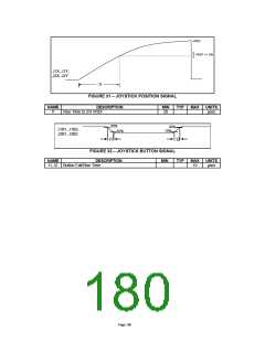
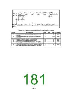
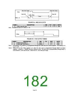
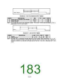
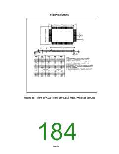
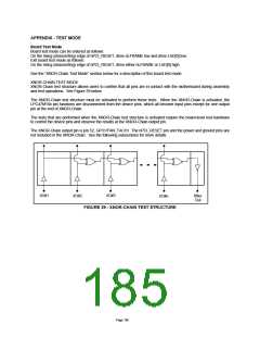
Introduction
The LPC47M10x provides board test capability through the XNOR chain. When the chip is in the XNOR chain test
mode, setting the state of any of the input pins to the opposite of its current state will cause the output of the chain to
toggle.
All pins on the chip are inputs to the XNOR chain, with the exception of the following:
1. VCC (pins 53, 65 & 93), VTR (pin 18), and VREF (pin 44).
2. VSS (pins 7, 31, 60, & 76) and AVSS (pin 40).
3. FAN_TACH1 (pin 52). This is the chain output.
4. nPCI_RESET (pin 26).
To put the chip in the XNOR chain test mode, tie LAD0 (pin 20) and nLFRAME (pin 24) low. Then toggle
nPCI_RESET (pin 26) from a low to a high state. Once the chip is put into XNOR chain test mode, LAD0 (pin 20) and
nLFRAME (pin 24) become part of the chain.
To exit the XNOR chain test mode tie LAD0 (pin 20) or nLFRAME (pin 24) high. Then toggle nPCI_RESET (pin 26)
from a low to a high state. A VCC POR will also cause the XNOR chain test mode to be exited. To verify the test
mode has been exited, observe the output at FAN_TACH1 (pin 52). Toggling any of the input pins should not cause
its state to change.
Setup
Warning: Ensure power supply is off during setup.
1. Connect VSS (pins 7, 31, 60, & 76) and AVSS (pin 40) to ground.
2. Connect VCC (pins 53, 65 & 93), VTR (pin 18), and VREF (pin 44) to VCC (3.3V).
3. Connect an oscilloscope or voltmeter to FAN_TACH1 (pin 52).
4. All other pins should be tied to ground.
Testing
1. Turn power on.
2. With LAD0 (pin 20) and nLFRAME (pin 24) low, bring nPCI_RESET (pin 26) high. The chip is now in XNOR
chain test mode. At this point, all inputs to the XNOR chain are low. The output, on FAN_TACH1 (pin 52),
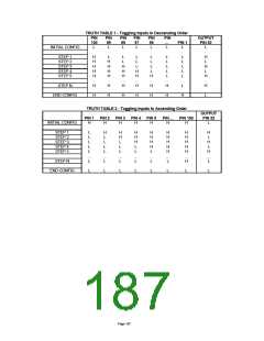
should also be low. Refer to INITIAL CONFIG on Truth Table 1.
3. Bring pin 100 high. The output on FAN_TACH1 (pin 52) should go high. Refer to STEP ONE on Truth Table
1.
4. In descending pin order, bring each input high. The output should switch states each time an input is
toggled. Continue until all inputs are high. The output on FAN_TACH1 should now be low. Refer to END
CONFIG on Truth Table 1.
5. The current state of the chip is now represented by INITIAL CONFIG in Truth Table 2.
6. Each input should now be brought low, starting at pin one and continuing in ascending order. Continue until
all inputs are low. The output on FAN_TACH1 should now be low. Refer to Truth Table 2.
7. To exit test mode, tie LAD0 (pin 20) OR nLFRAME (pin 24) high, and toggle nPCI_RESET from a low to a
high state.
Page 186

 SMSC [ SMSC CORPORATION ]