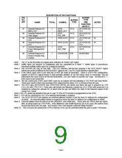
Buffer Type Descriptions
Note: The buffer type values are specified at VCC=3.3V
IO12
IS/O12
O12
Input/Output, 12mA sink, 6mA source.
Input with Schmitt Trigger/Output, 12mA sink, 6mA source.
Output, 12mA sink, 6mA source.
OD12
O6
Open Drain Output, 12mA sink.
Output, 6mA sink, 3mA source.
O8
Output, 8mA sink, 4mA source.
OD14
OP14
IOP14
IS/OP14
IOD16
O4
Open Drain Output, 14mA sink.
Output, 14mA sink, 14mA source.
Input/Output, 14mA sink, 14mA source. Backdrive protected.
Input with Schmitt Trigger/Output, 14mA sink, 14mA source, Backdrive Protected.
Input/Output (Open Drain), 16mA sink.
Output, 4mA sink, 2mA source.
IO8
Input/Output, 8mA sink, 4mA source.
I
Input TTL Compatible.
IS
Input with Schmitt Trigger.
PCI_IO
PCI_O
PCI_OD
Input/Output. These pins must meet the PCI 3.3V AC and DC Characteristics. (Note 1)
Output. These pins must meet the PCI 3.3V AC and DC Characteristics. (Note 1)
Open Drain Output. These pins must meet the PCI 3.3V AC and DC Characteristics.
(Note 1)
PCI_I
PCI_ICLK
Input. These pins must meet the PCI 3.3V AC and DC Characteristics. (Note 1)
Clock Input. These pins must meet the PCI 3.3V AC and DC Characteristics and timing. (Note 2)
Note 1. See the PCI Local Bus Specification, Revision 2.1, Section 4.2.2.
Note 2. See the PCI Local Bus Specification, Revision 2.1, Section 4.2.2. and 4.2.3.
Page 10

 SMSC [ SMSC CORPORATION ]